Supercharge Your Innovation With Domain-Expert AI Agents!

Chip packaging structure and manufacturing method thereof

A technology of chip packaging structure and manufacturing method, which is applied in the directions of antenna support/installation device, semiconductor/solid-state device manufacturing, electrical components, etc. problems, such as heat dissipation problems of high-level packaging, to achieve the effect of extending the service life

Pending Publication Date: 2021-07-23
UNIMICRON TECH CORP
View PDF0 Cites 0 Cited by
  • Summary
  • Abstract
  • Description
  • Claims
  • Application Information

AI Technical Summary

Problems solved by technology

Therefore, in the above-mentioned manufacturing method, it is impossible to add heat dissipation blocks or heat dissipation fins to dissipate heat from the chip, so it is impossible to solve the heat dissipation problem of the fan-out multi-band antenna wafer level package.

Method used


Image

  • Chip packaging structure and manufacturing method thereof
  • Chip packaging structure and manufacturing method thereof
  • Chip packaging structure and manufacturing method thereof

Examples


Embodiment Construction

[0064] Reference will now be made in detail to the exemplary embodiments of the present invention, examples of which are illustrated in the accompanying drawings. Wherever possible, the same reference numbers will be used in the drawings and description to refer to the same or like parts.

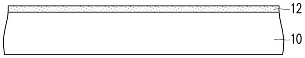
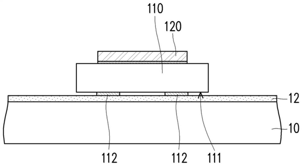
[0065] Figure 1A to Figure 1J It is a schematic cross-sectional view of a manufacturing method of a chip packaging structure according to an embodiment of the present invention. figure 2 for Figure 1J A schematic top view of the chip package structure. Regarding the manufacturing method of the chip package structure of this embodiment, first, please refer to Figure 1A , providing the carrier 10 on which the adhesive layer 12 has been formed. Here, the adhesive layer 12 is, for example, a double-sided thermal release tape, but not limited thereto.

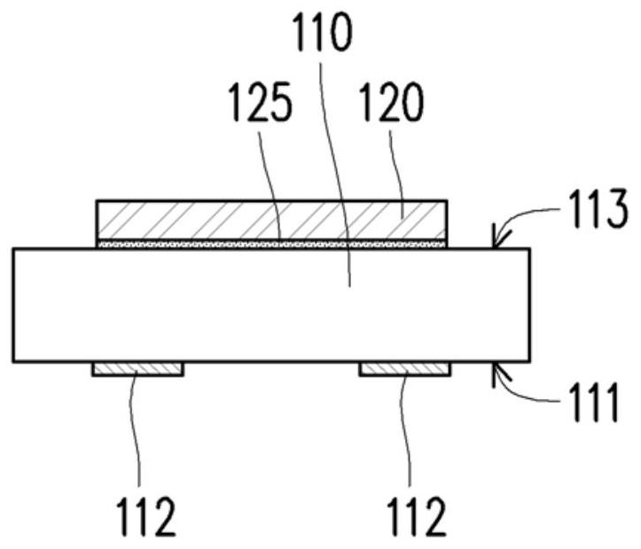
[0066] Next, please refer to Figure 1B , provide at least one chip (a chip 110 is schematically shown) and at least one heat conductio...


PUM


Abstract

The invention provides a chip packaging structure and a manufacturing method thereof. The chip packaging structure comprises at least one chip, at least one heat conduction element, a packaging colloid and a reconfiguration circuit layer. Each chip has an active surface and a back surface opposite to each other, and a plurality of electrodes disposed on the active surface. The heat conduction element is arranged on the back surface of each chip. The packaging colloid wraps the chip and the heat conduction element and is provided with an upper surface and a lower surface which are opposite to each other. The bottom surface of each electrode of each chip is aligned with the lower surface of the packaging colloid. The packaging colloid exposes the top surface of each heat conduction element. The reconfiguration circuit layer is disposed on the lower surface of the packaging colloid and electrically connected to the electrode of each chip.

Description

technical field [0001] The invention relates to a packaging structure and a manufacturing method thereof, in particular to a chip packaging structure and a manufacturing method thereof. Background technique [0002] The fan-out multi-band antenna wafer-level packaging design can miniaturize the electronic circuit and greatly reduce the electrical insertion loss. As the transmission frequency and operation speed of electronic products become faster and faster in the future, the accompanying problem of chip heat dissipation will become more and more important. However, in the fabrication of the aforementioned fan-out multi-band antenna WLP, the active surface of the chip is face-up to be back-bonded to the first reconfiguration circuit layer as the ground pattern of the antenna, and then A second reconfiguration circuit layer electrically connected to solder balls is formed on the active surface of the chip. Therefore, in the above-mentioned manufacturing method, it is impos...

Claims


Application Information

Patent Timeline
Patent Type & Authority Applications(China)
IPC IPC(8): H01L23/31H01L23/367H01L23/498H01L23/66H01L21/48H01L21/56H01Q1/22
CPCH01L23/3114H01L23/367H01L23/49811H01L23/49838H01L23/66H01L21/56H01L21/4853H01Q1/2283
Inventor 刘汉诚沈裕琪曾子章郑振华王佰伟
Owner UNIMICRON TECH CORP
Features
  • R&D
  • Intellectual Property
  • Life Sciences
  • Materials
  • Tech Scout
  • Unparalleled Data Quality
  • Higher Quality Content
  • 60% Fewer Hallucinations
Learn More