Non-photopolymerization PCB solder resist ink windowing and solder resist oil bridge process

A technology of solder resist ink and PCB board, which is applied in pattern and photolithography, coating of non-metallic protective layer, electrical components, etc., can solve the problem of low resolution of solder resist ink, inability to completely retain solder resist oil bridge, and impurity virtual soldering and other problems, to achieve the effect of solving poor welding and solving the problem of solder mask window deviation

Inactive Publication Date: 2021-07-23
东莞市春瑞电子科技有限公司
View PDF4 Cites 5 Cited by
  • Summary
  • Abstract
  • Description
  • Claims
  • Application Information

AI Technical Summary

Problems solved by technology

[0003] 1. Due to the difference in expansion and shrinkage of the plate and film film during the production process of the PCB board 1, there will be alignment problems with the PCB board 1 when transferring the pattern of the solder resist ink window 5;
[0004] 2. When the PCB board 1 is transferring the circuit and solder resist ink graphics, there is a problem of accuracy error of the alignment equipment;
[0005] 3. In the existing production process, in order to deal with the problem of the precision of the window 5 of the solder resist ink, the size a of the window 5 of the solder resist ink will be larger than the size b of the pad 2, and the reserved space on one side needs to be more than 30 microns, and There is still the risk of solder resist ink 3 on pad 2 caused by the deviation of the pattern of solder resist ink window 5;
[0006] 4. This method of opening the window 5 of the solder resist will cause the solder resist oil bridge 4 not to be in contact with the pad 2, and only one end is connected to the PCB board 1. The ink has low adhesion and is easy to fall off, which can easily cause a short circuit of the tin and the pad during soldering. Welding of impurities;
[0007] 5. The existing production process needs to increase the window 5 graphics, coupled with the low resolution of the solder mask ink and the characteristics of embrittlement after drying and curing, it is impossible to completely retain the solder mask for pads with a pad spacing of less than 0.15mm Oil bridge 4; especially for the current high-precision micro components, the distance between solder pins is less than 0.1mm, the existing production process can only directly open the window, and there is no solder resist oil bridge 4 barrier between solder pins, which is extremely Greatly increased the defect rate and scrap rate of the product

Method used


Image

  • Non-photopolymerization PCB solder resist ink windowing and solder resist oil bridge process
  • Non-photopolymerization PCB solder resist ink windowing and solder resist oil bridge process
  • Non-photopolymerization PCB solder resist ink windowing and solder resist oil bridge process

Examples


Embodiment Construction

[0029] The following will clearly and completely describe the technical solutions in the embodiments of the present invention in conjunction with the accompanying drawings in the embodiments of the present invention,

[0030] Please refer to Figure 2-4 ,

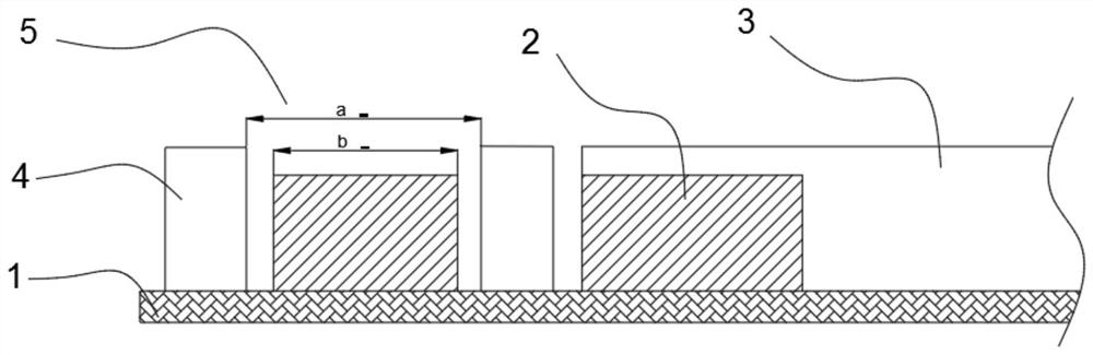
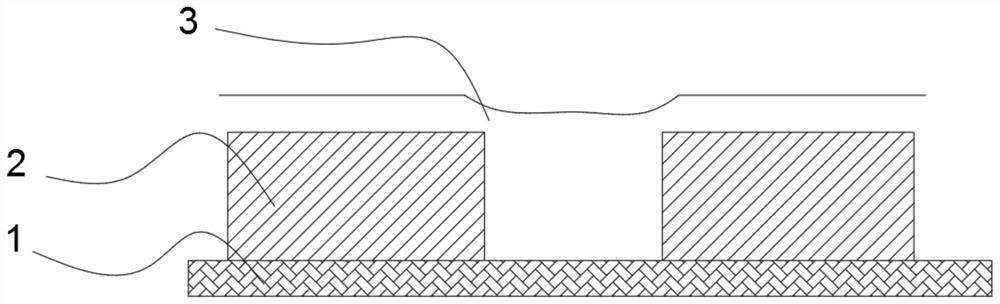
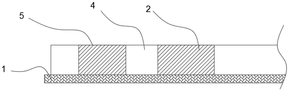
[0031] A non-photopolymerizable PCB solder resist ink window opening and solder resist oil bridge process, used for high-precision PCB micro pads 2 solder resist ink 3 window opening 5, solder resist oil bridge 4 production,

[0032] S1: Make the blocking screen

[0033] Choose a screen printing screen with a mesh size of 43T and a tension of 24N. According to the hole position information of the PCB board 1 to be produced, print the corresponding block film graphics on the screen (except for the holes that need to be plugged). clogged.

[0034] S2: Screen printing ink

[0035] Install the stencil with the stop point on the double scraper automatic screen printing machine, fix the PCB board 1 position according to the s...


PUM

PropertyMeasurementUnit
thicknessaaaaaaaaaa

Abstract

The invention discloses a non-photopolymerization PCB solder resist ink windowing and solder resist oil bridge process, which is used for high-precision PCB micro bonding pad solder resist ink windowing and solder resist oil bridge, and comprises the following steps of S1, manufacturing a blocking point screen, S2, silk-screening ink, S3, carrying out pre-baking treatment, S4, carrying out ink leveling treatment, and leveling the pre-baked solder resist ink by adopting an ink leveling machine, S5, drying and curing treatment: carrying out high-temperature drying and curing on the printed circuit board with the ink leveled, S6, grinding treatment: grinding the ink on the copper surface of the bonding pad to completely expose the copper layer of the bonding pad, and S7, cleaning and drying treatment: cleaning and drying the ground PCB through a horizontal surface cleaning machine, and carrying out micro-etching leveling and cleaning on the exposed copper surface by using a micro-etching leveling liquid and high-pressure water. The process is suitable for any-sizepad windowing and solder resist oil bridge manufacturing, and a powerful quality guarantee is provided for electronic products which are more and more integrated and precise.

Description

technical field [0001] The invention belongs to the technical field of PCB board production and processing, in particular to a non-photopolymerizable PCB solder resist ink window opening and solder resist oil bridge process. Background technique [0002] The solder resist ink window opening and solder resist oil bridge process used in the prior art mainly uses film negatives to complete the transfer of the solder resist ink window opening pattern through UV ultraviolet light polymerization and alkaline developing liquid washing process. However, due to the limitations of the accuracy of material expansion and contraction and the low-resolution characteristics of solder resist inks in this process, the following shortcomings exist in the production of solder resist inks for PCB boards. figure 1 Shown: [0003] 1. Due to the difference in expansion and contraction of the plate and the film film during the production process of the PCB board 1, there will be alignment problems...

Claims


Application Information

Patent Timeline
Patent Type & Authority Applications(China)
IPC IPC(8): H05K3/28
CPCH05K3/285H05K2203/0571
Inventor 钟峰周志国
Owner 东莞市春瑞电子科技有限公司
Why Eureka
Try Eureka