

Semiconductor storage device
A storage device and semiconductor technology, applied in the field of semiconductors, can solve problems such as small area of semiconductor memory
Active Publication Date: 2021-07-27
CHANGXIN MEMORY TECH INC
View PDF10 Cites 0 Cited by
- Summary
- Abstract
- Description
- Claims
- Application Information
AI Technical Summary
Problems solved by technology
[0005] The present application provides a semiconductor storage device to solve the problem of how to make the semiconductor storage area smaller and smaller
Method used
View moreImage
Smart ImageViewing Examples

Examples
Embodiment 1
Login to View More PUM
 Abstract
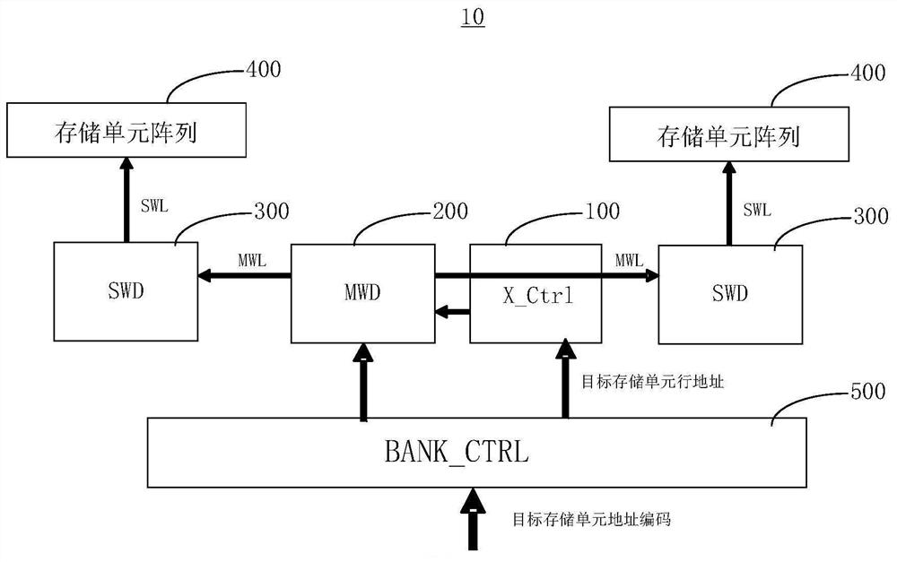
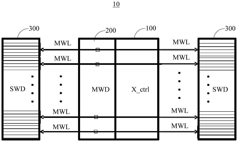
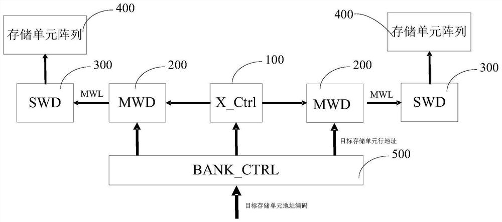
The invention provides a semiconductor storage device. The semiconductor storage device comprises a decoding module, a main word line driving module, a sub word line driving module and a storage unit array, the decoding module is configured to decode a target storage unit row address to generate a main word line selection signal and a sub word line selection signal; a main word line driving module configured to drive a plurality of main word lines in response to a main word line selection signal; the sub-word line driving module is configured to respond to a sub-word line selection signal to drive a plurality of sub-word lines; one memory cell array comprises a plurality of memory cells, the sub-word line driving module is arranged at the edge of any side of the memory cell array, and the output end of the sub-word line driving module is connected with a word line of the memory cell array; at least two different memory cell arrays share one group of main word line driving modules, and one decoding module is connected with at least one group of main word line driving modules. The semiconductor storage device provided by the invention is smaller in area and better meets the use requirements of a semiconductor memory.
Description
technical field [0001] The present application relates to semiconductor technology, and in particular to a semiconductor storage device. Background technique [0002] A semiconductor memory device, especially a Dynamic Random Access Memory (DRAM for short) is designed such that a main word line selectively activates one of a plurality of sub-word lines. For example, when there are 64 main word lines and sub word lines exist for each main word line, one main word line activates one of 8 sub word lines. [0003] When reading information from the DRAM memory, it is necessary to know the address code of the storage unit corresponding to the information to be read, and then read the corresponding row code of the storage unit according to the address code of the storage unit, and activate the corresponding word according to the row code of the storage unit. Wire. After the word line is activated, the memory cells connected to the word line are in a readable and writable state. ...
Claims
Login to View More Application Information
Patent Timeline
 Patent Type & AuthorityApplications(China)
IPC IPC(8): G11C11/408G11C11/4063
CPCG11C11/4085G11C11/4063
Inventor孙会娟李智勋
OwnerCHANGXIN MEMORY TECH INC