Equipment and method for determining height of semiconductor structure

A semiconductor and advanced technology, applied in semiconductor/solid-state device manufacturing, semiconductor/solid-state device testing/measurement, electrical components, etc., it can solve the problems of limited measurement quantity, large measurement error, poor measurement stability, etc., to improve sealing, Improved balance and improved accuracy

Active Publication Date: 2021-08-13
徐州博创建设发展集团有限公司
View PDF6 Cites 2 Cited by
  • Summary
  • Abstract
  • Description
  • Claims
  • Application Information

AI Technical Summary

Problems solved by technology

[0005] The purpose of the present invention is to solve the problem that when measuring the average height of semiconductors, it is mostly measured manually and then averaged, but the number of manual single measurements is limited, and the measurement efficiency is slow. When measuring multiple semiconductors at a time, the measurement is stable. Poor, the measurement error is large, resulting in a large error in the average value of the semiconductor, which affects the accuracy of the average value

Method used


Image

  • Equipment and method for determining height of semiconductor structure
  • Equipment and method for determining height of semiconductor structure
  • Equipment and method for determining height of semiconductor structure

Examples


Embodiment 1

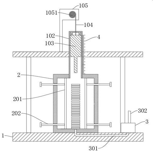
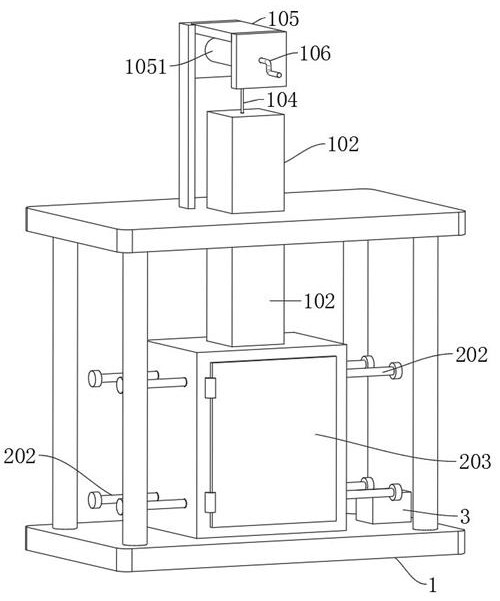
[0039] refer to Figure 1-8 , the equipment used to determine the height of the semiconductor structure, including a mounting frame 1, also includes: a negative pressure box 2, fixedly connected to the mounting frame 1, wherein, one side of the negative pressure box 2 is provided with an opening 306; the box door 203, rotating Connected to the opening 306; the sleeve 102 is fixedly connected to the top of the negative pressure box 2, and one end communicates with the negative pressure box 2, wherein the sleeve 102 is made of transparent material; the measuring scale 4 is arranged on the sleeve 102; the measuring rod 103, slidingly connected in the sleeve 102; stay rope 104, one end is fixedly connected to the top of the measuring rod 103, and the other end runs through the outside of the sleeve 102; the sliding plate 201 is symmetrically slidingly connected in both sides of the negative pressure box 2; the negative pressure pump 3. It is fixedly connected to the installation f...

Embodiment 2

[0054] refer to figure 1 , 2 and 6, which are basically the same as in Embodiment 1, furthermore: a guide rod 202 is fixedly connected to the sliding plate 201, and the end of the guide rod 202 away from the sliding plate 201 slides through and slides on the negative pressure box 2;

[0055] The guide rod 202 can provide a position-limiting guiding effect on the sliding plate 201 when sliding, so as to prevent the sliding plate 201 from being unable to slide due to uneven force when sliding;

[0056] After the measurement is completed, open the box door 203, take out the semiconductor, and then push the two sets of sliding plates 201 away from each other to expand the area for placing the semiconductor next time.

Embodiment 3

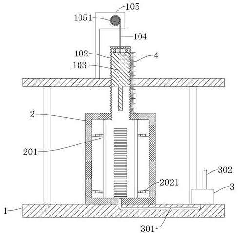
[0058] refer to image 3 , which is basically the same as in Embodiment 1, furthermore: the sliding plate 201 is fixedly connected to a multi-stage telescopic rod 2021, and the end of the multi-stage telescopic rod 2021 away from the sliding plate 201 is fixedly connected to the inner wall of the negative pressure box 2;

[0059] When the sliding plate 201 slides, the multi-stage telescopic rod 2021 is pulled to elongate, and the multi-stage telescopic rod 2021 also plays a role of limiting and guiding the sliding plate 201;

[0060] After the measurement is completed, open the box door 203, take out the semiconductor, and push the two sets of sliding plates 201 away from each other. When the sliding plates 201 are pushed, the multi-stage telescopic rod 2021 will shrink accordingly;

[0061] However, the multi-stage telescopic rod 2021 is arranged in the negative pressure box 2 and does not penetrate the negative pressure box 2, so that the airtightness of the negative pressur...


PUM


Abstract

The invention discloses equipment and a method for determining the height of a semiconductor structure, and belongs to the technical field of semiconductors. The equipment for determining the height of the semiconductor structure comprises a mounting rack and further comprises a negative pressure box fixedly connected to the mounting rack, wherein one side of the negative pressure box has an opening; a box door which is rotationally connected to the opening; and a sleeve which is fixedly connected to the top part of the negative pressure box, wherein one end of the sleeve is communicated with the negative pressure box, and the sleeve is made of a transparent material. By adopting the equipment, a plurality of semiconductors can be measured at a time through using a stacking method, the average height value of the semiconductors of the same batch and the same model is further obtained, the semiconductors are limited through the sliding plate during measurement, the stability of the semiconductors during measurement is improved, the measurement precision is further improved, and the average value is calculated by reading the measurement scales; and the equipment is convenient, fast, high in measurement efficiency and high in measurement accuracy.

Description

technical field [0001] The invention relates to the technical field of semiconductors, in particular to equipment and methods for determining the height of semiconductor structures. Background technique [0002] A conductor is a substance whose conductivity is between an insulator and a conductor. Its conductivity is easy to control and can be used as a component material for information processing. From the perspective of technology or economic development, semiconductors are very important; many electronic products, such as The core units of computers, mobile phones, and digital recorders all use semiconductor conductivity changes to process information; [0003] After the same batch of semiconductors of the same type are produced, they will enter the next process for packaging. In order to improve efficiency during packaging, the semiconductors will be placed in the positioning slots to quickly position the semiconductors, and then the packaging machine will drive the chi...

Claims


Application Information

Patent Timeline
Patent Type & Authority Applications(China)
IPC IPC(8): H01L21/66H01L21/67
CPCH01L21/67121H01L22/12
Inventor 闫长春
Owner 徐州博创建设发展集团有限公司
Why Eureka
Try Eureka