Semiconductor lead frame punch forming product discharging, stacking and transferring device

A technology of lead frame and transfer device, which is applied in the stacking, transportation and packaging of objects, and can solve the problems of unfavorable lean production management, time required, and time increase, so as to avoid damage and scrap, improve stability, and be practical sex enhancing effect

A technology of lead frame and transfer device, which is applied in the stacking, transportation and packaging of objects, and can solve the problems of unfavorable lean production management, time required, and time increase, so as to avoid damage and scrap, improve stability, and be practical sex enhancing effect

CN111994640AActive Publication Date: 2020-11-27四川富美达微电子有限公司

Image

  • Semiconductor lead frame punch forming product discharging, stacking and transferring device
  • Semiconductor lead frame punch forming product discharging, stacking and transferring device
  • Semiconductor lead frame punch forming product discharging, stacking and transferring device

Examples


Embodiment

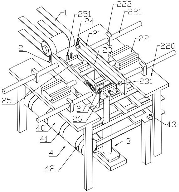
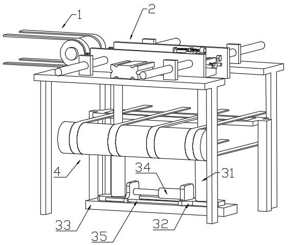
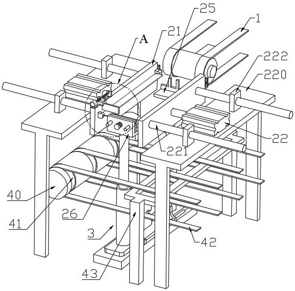
[0032] Such as Figure 1~6 As shown in the example, a semiconductor lead frame stamping and forming product discharge stacking transfer device used in this example is set at the end of the discharge conveyor belt 1 of the lead frame stamping die, including: a carrying mechanism 2, a lifting mechanism 3, and a transfer mechanism 4 Wait.

[0033] The carrying mechanism 2 is used to carry the finished lead frame products conveyed from the discharge conveyor belt 1. The carrying mechanism 2 includes a pair of space-adjustable limit plates 21 and a first L spaced between the limit plates 21 and oppositely arranged. Type bearing plate 25 and the second L-shaped bearing plate 26.

[0034] The lifting mechanism 3 is connected to the first L-shaped loading plate 25 and the second L-shaped loading plate 26 for driving the first L-shaped loading plate 25 and the second L-shaped loading plate 26 to lift.

[0035] The conveying direction of the transfer mechanism 4 is perpendicular to th...


PUM


Abstract

The invention discloses a semiconductor lead frame punch forming product discharging, stacking and transferring device. The semiconductor lead frame punch forming product discharging, stacking and transferring device comprises a bearing mechanism, a lifting mechanism and a transferring mechanism, wherein the bearing mechanism comprises a pair of spacing-adjustable limiting plates, a first L-shapedbearing plate and a second L-shaped bearing plate, and the first L-shaped bearing plate and the second L-shaped bearing plate are oppositely arranged at an interval between the limiting plates; the lifting mechanism is connected with the first L-shaped bearing plate and the second L-shaped bearing plate and used for driving the first L-shaped bearing plate and the second L-shaped bearing plate toascend and descend; and the conveying direction of the transferring mechanism is perpendicular to the conveying direction of a discharging conveying crawler belt, the transferring mechanism comprisesa rotating roller and a plurality of conveying belts arranged on the rotating roller at intervals, and the first L-shaped bearing plate and the second L-shaped bearing plate are located at the intervals of the pair of adjacent conveying belts correspondingly. According to the device, stamped and formed lead frames can be stacked in order, the influence of a height difference at the moment when adischarged material is separated from a conveying crawler belt on the lead frames is avoided, slow descending stacking is achieved, and the lead frames stacked to the designated height can be conveyedto the rear stage in order after being stacked in order.

Description

technical field [0001] The invention relates to the field of semiconductor components, in particular to a device for stacking and transferring semiconductor lead frame stamped products. Background technique [0002] Lead frame is an important carrier of semiconductor devices and integrated circuit modules. In the preparation of this type of device / module, the required wafer / chip is usually fixed on the designated area of ​​the lead frame by means of bonding, etc., and electrical conduction is achieved by bonding gold wires or setting jumpers, and then packaged. Plastic base, and corresponding cutting, punching, folding, etc. to obtain products. [0003] In the preparation of the lead frame, it is necessary to use a mold to perform stamping or pressing of different shapes on the designated areas of the lead frame, so as to obtain the finished lead frame. Usually, after the lead frame is formed, it is sent out by the crawler conveyor mechanism, and then the material is simpl...

Claims


Application Information

Patent Timeline
27 Nov 2020
Publication
CN111994640A
IPC
B65G57/11
CPC
B65G57/11
Inventors
曾尚文; 陈久元