Electric leakage test structure and electric leakage test method

A test structure and test method technology, applied in the field of integrated circuit manufacturing, can solve problems such as parasitic leakage that cannot reflect the internal design of semiconductor devices

Active Publication Date: 2021-08-13
GUANGZHOU CANSEMI TECH INC
View PDF5 Cites 1 Cited by
  • Summary
  • Abstract
  • Description
  • Claims
  • Application Information

AI Technical Summary

Problems solved by technology

[0004] The purpose of the present invention is to provide a leakage test structure and a leakage test method to solve the problem th

Method used


Image

  • Electric leakage test structure and electric leakage test method
  • Electric leakage test structure and electric leakage test method
  • Electric leakage test structure and electric leakage test method

Examples


Embodiment Construction

[0022] The leakage test structure and leakage test method proposed by the present invention will be further described in detail below in conjunction with the accompanying drawings and specific embodiments. The advantages and features of the present invention will become clearer from the following description. It should be noted that all the drawings are in a very simplified form and use imprecise scales, and are only used to facilitate and clearly assist the purpose of illustrating the embodiments of the present invention.

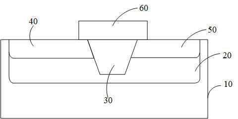
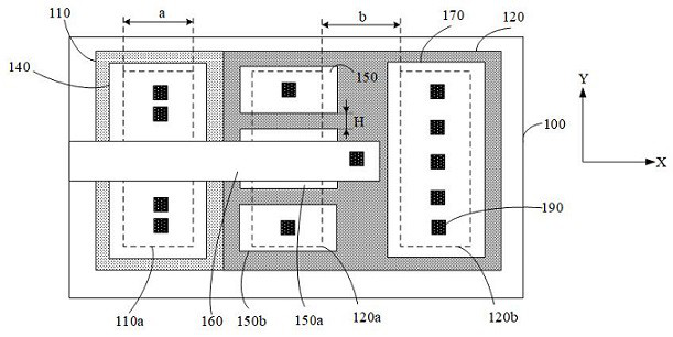
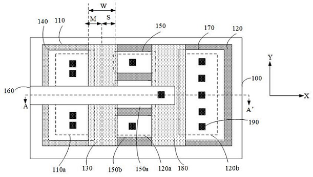
[0023] figure 2 It is a top view of the leakage test structure not including the first shallow trench isolation structure and the second shallow trench isolation structure provided by the embodiment of the present invention, image 3 It is a top view of the leakage test structure including the first shallow trench isolation structure and the second shallow trench isolation structure provided by the embodiment of the present invention, namely figure 2 T...


PUM


Abstract

The invention provides an electric leakage test structure and an electric leakage test method. the electric leakage test structure comprises a substrate, and a first well region and a second well region are formed in the substrate; and the electric leakage test structure further comprises a first shallow trench isolation structure formed between the second well region and the first well region, a first source and drain region formed in the first well region, a plurality of second source and drain regions formed in the second well region and a test grid electrode formed on the substrate. In the electric leakage test method, the design sizes of the plurality of electric leakage test structures are different, and each electric leakage test structure is tested, so that the leakage current in each electric leakage test structure can be obtained; and the corresponding relation between the design size and the leakage current in the electric leakage test structure is obtained according to the leakage current in each electric leakage test structure, so that the problems of parasitic electric leakage and the like caused by the internal design of the semiconductor device can be reflected.

Description

technical field [0001] The invention relates to the technical field of integrated circuit manufacturing, in particular to a leakage test structure and a leakage test method. Background technique [0002] Semiconductor technology In the design of integrated circuits or the development of process technology platforms, it is usually necessary to use a variety of leakage test structures to reflect whether the circuit design and process capabilities of semiconductor devices are normal. Different leakage test structures can reflect different device characteristics. The characteristics improve circuit design or process in semiconductor devices. Leakage is a problem that cannot be ignored in semiconductor devices, especially the parasitic leakage of semiconductor devices. [0003] When testing the leakage of semiconductor devices, usually such as figure 1 The leakage test structure shown (more leakage test structures currently used in the industry), the leakage test structure incl...

Claims


Application Information

Patent Timeline
IPC IPC(8): H01L23/544H01L21/66G01R31/52
CPCH01L22/34H01L23/544H01L22/14H01L22/20G01R31/52
Inventor 陈泽勇周正良
Owner GUANGZHOU CANSEMI TECH INC
Why Eureka
Try Eureka