
Chip mounter anti-chip-floating detection device and method

A detection device and chip mounter technology, which is applied to measurement devices, optical devices, instruments, etc., can solve the problems of chipping of silicon wafers, economic losses, damage to polishing pads, ceramic disc polishing machines, etc., to achieve easy operation, The effect of reducing maintenance man-hours and avoiding economic losses

Pending Publication Date: 2021-08-17
ZHONGHUAN ADVANCED SEMICON MATERIALS CO LTD +1
View PDF0 Cites 1 Cited by
  • Summary
  • Abstract
  • Description
  • Claims
  • Application Information

AI Technical Summary

Problems solved by technology

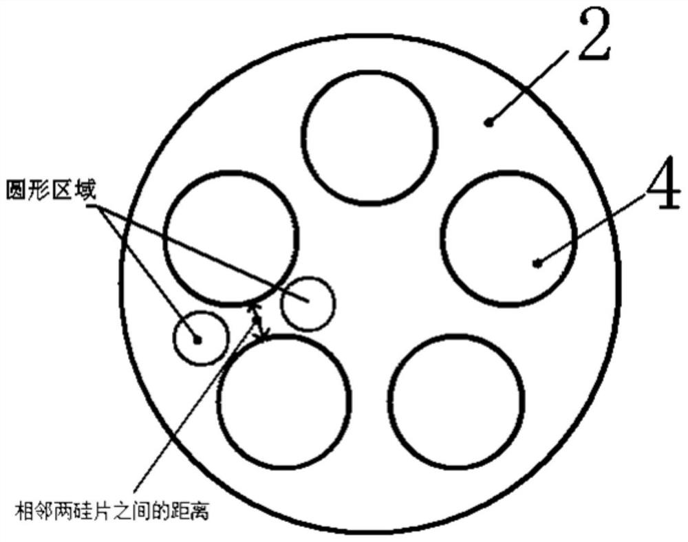
[0002] At present, when polishing silicon wafers, it is necessary to paste multiple silicon wafers on the ceramic plate according to certain rules. If there is a position deviation in the position of the paste, or even two silicon wafers are overlapped or overlapped, they will be stuck together. During the polishing process, silicon wafers are broken, and polishing pads, ceramic discs, center guide wheels, side guide wheels, polishing machine plates and other components are damaged, resulting in huge economic losses

Method used


Image

  • Chip mounter anti-chip-floating detection device and method
  • Chip mounter anti-chip-floating detection device and method
  • Chip mounter anti-chip-floating detection device and method

Examples


Embodiment Construction

[0042] It should be noted that, in the case of no conflict, the embodiments of the present invention and the features in the embodiments can be combined with each other.

[0043] The present invention will be described in detail below with reference to the accompanying drawings and examples.

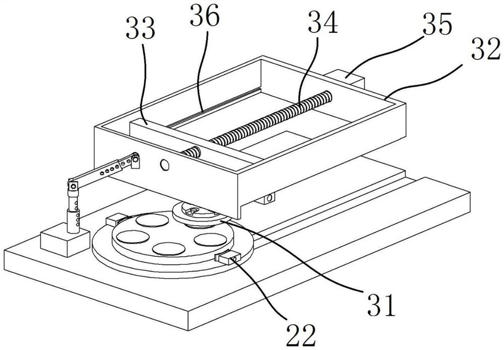
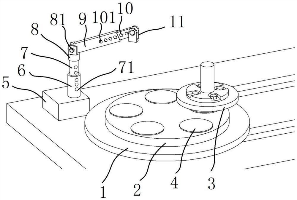
[0044] Such as Figure 1 to Figure 7 As shown, a chip mounter 3 anti-floating detection device includes a ceramic disk 2, a chip mounter 3 and an image acquisition unit. The upper surface of the ceramic disk 2 forms a placement area for placing a silicon chip 4, and the chip mounter 3 is set Above the ceramic disc 2, it is used to place a silicon chip 4 on the ceramic disc 2;

[0045] The image acquisition unit includes a camera and an image processing system, the camera is arranged above the ceramic disc 2, and the camera is connected with the image processing system.

[0046] It also includes a base 1. The ceramic disc 2 is placed on the upper surface of the base 1. The ceramic disc ...


PUM


Abstract

The invention provides a chip mounter anti-chip-floating detection device and method. The device comprises a ceramic disc, a chip mounter and an image acquisition unit. The upper surface of the ceramic disc forms a placement area for placing silicon chips, and the chip mounter is arranged above the ceramic disc and is used for placing the silicon chips on the ceramic disc; the image acquisition unit comprises a camera and an image processing system, the camera is arranged above the ceramic plate, and the camera is connected with the image processing system. The device and method have the advantages that the chip fluttering prevention detection function of the chip mounter is added, and the chip mounter chip fluttering prevention detection device and method are easy to manufacture, low in failure rate, safe, reliable and convenient to operate; according to the actual use effect of a workshop site, the system can effectively avoid silicon wafer fragmentation and damage to parts such as a polishing pad, a ceramic disc, a center guide wheel, a side guide wheel and a polishing machine large disc caused by chip fluttering of the chip mounter, avoids huge economic loss and reduces maintenance man hours.

Description

technical field [0001] The invention belongs to the technical field of silicon wafer processing, and in particular relates to an anti-floating wafer detection device and method of a placement machine. Background technique [0002] At present, when polishing silicon wafers, it is necessary to paste multiple silicon wafers on the ceramic plate according to certain rules. If there is a position deviation in the position of the paste, or even two silicon wafers are overlapped or overlapped, they will be stuck together. During the polishing process, silicon wafers are broken, and polishing pads, ceramic discs, center guide wheels, side guide wheels, polishing machine plates and other components are damaged, resulting in huge economic losses. Contents of the invention [0003] In view of this, the present invention aims to propose a chip mounter anti-floating chip detection device and method, in order to prevent the silicon chip from being biased or stacked during the chip mount...

Claims


Application Information

Patent Timeline
Patent Type & Authority Applications(China)
IPC IPC(8): G01B11/00
CPCG01B11/00Y02P70/50
Inventor 李文磊严政先安爱博赵欣郭会波刘子申孙晨光王彦君
Owner ZHONGHUAN ADVANCED SEMICON MATERIALS CO LTD
Learn More