A differential voltage detection circuit with wide voltage input range

A wide voltage input, differential voltage technology, applied in the field of integrated circuits, can solve the problems of small input offset voltage and narrow voltage input range, and achieve the effect of reducing input offset voltage and strong practicability

Active Publication Date: 2022-08-02
晶通微电子(南京)有限公司
View PDF15 Cites 0 Cited by
  • Summary
  • Abstract
  • Description
  • Claims
  • Application Information

AI Technical Summary

Problems solved by technology

[0006] The embodiment of the present application solves the technical problem that the voltage input range of the voltage comparator or operational amplifier in the prior art is relatively narrow by providing a differential voltage detection circuit with a wide voltage input range, which can operate in a wide common-mode input voltage range It can also work in a wide differential mode input voltage range and has a small input offset voltage

Method used


Image

  • A differential voltage detection circuit with wide voltage input range
  • A differential voltage detection circuit with wide voltage input range
  • A differential voltage detection circuit with wide voltage input range

Examples


Embodiment 1

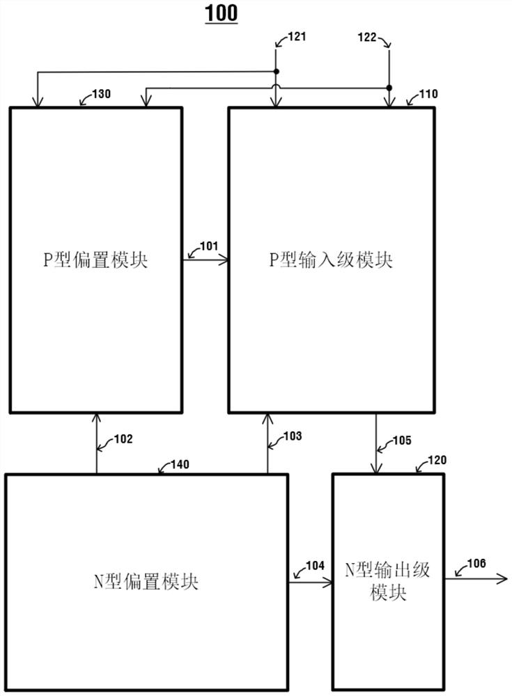
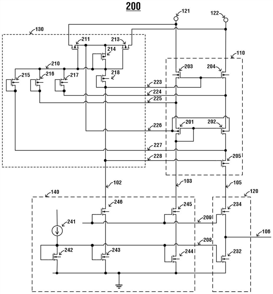
[0075] figure 2 It is a schematic diagram of a specific implementation circuit 200 of the differential voltage detection circuit with a wide voltage input range in this embodiment, wherein,

[0076] The P-type input stage module 110 includes a first PMOS transistor 201 , a second PMOS transistor 202 , a third PMOS transistor 203 , a fourth PMOS transistor 204 and a fifth PMOS transistor 205 . The third PMOS transistor 203 , the fourth PMOS transistor 204 and the fifth PMOS transistor 205 are high-voltage PMOS transistors, and the drains and sources of the high-voltage PMOS transistors can withstand voltages of tens of volts or even hundreds of volts.

[0077] The first PMOS transistor 201 and the second PMOS transistor 202 form a differential pair, and the gate of the first PMOS transistor 201 is connected to the gate of the second PMOS transistor 202 . The first PMOS transistor 201 and the second PMOS transistor 202 share the same N well on the chip layout, that is, they sh...

Embodiment 2

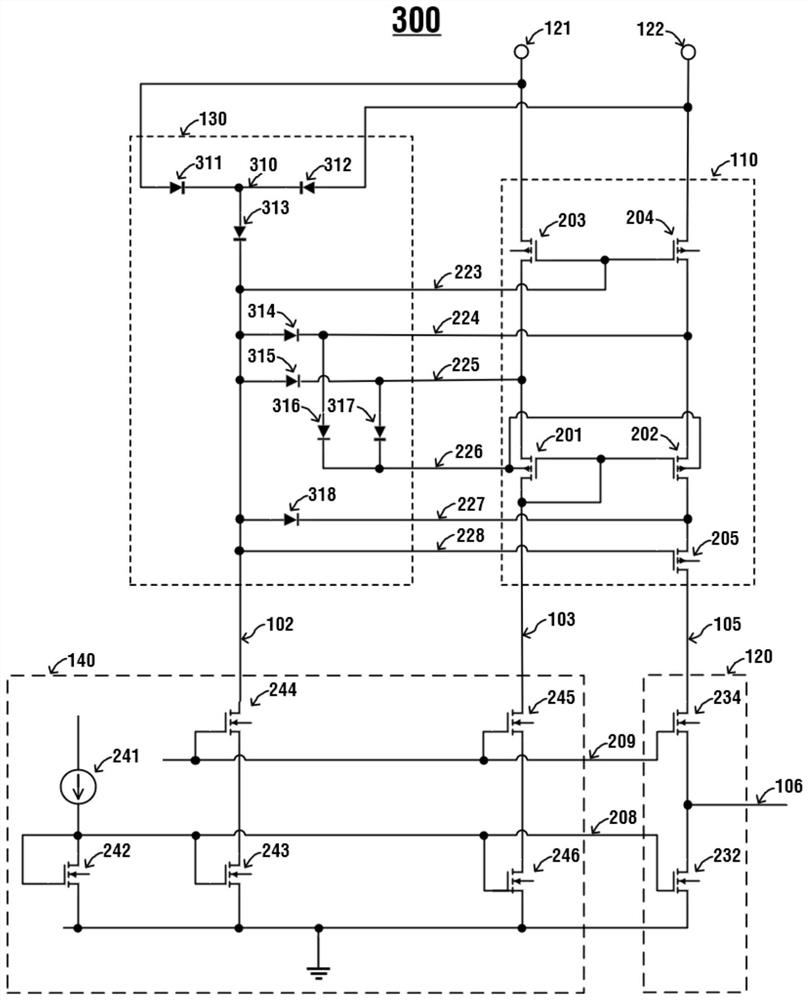
[0116] image 3 This is a schematic diagram of the specific implementation circuit of the differential voltage detection circuit with a wide voltage input range in the second embodiment of the application. The specific implementation circuit 300 of the differential voltage detection circuit with a wide voltage input range is different from the first embodiment only in that P Type bias module 130 . The function of the P-type bias module 130 is still to provide bias and clamping functions to the transistors inside the P-type input stage 110 .

[0117] The P-type bias module 130 includes a first diode 311, a second diode 312, a third diode 313, a fourth diode 314, a fifth diode 315, a sixth diode 316, a Seven diodes 317 and eighth diodes 318, wherein the first diode 311 and the second diode 312 are high voltage diodes.

[0118] The anode of the first diode 311 is connected to the first voltage input signal 121 , the anode of the second diode 312 is connected to the second volta...

Embodiment 3

[0125] Figure 4 This is a schematic diagram of the specific implementation circuit of the differential voltage detection circuit with a wide voltage input range in the third embodiment of the application. The specific implementation circuit 400 of the differential voltage detection circuit with a wide voltage input range is based on the third embodiment. optimization, the difference between it and the third embodiment is only: image 3 The sixth diode 316 and the seventh diode 317 in the middle P-type bias module 130 are Figure 4 is replaced by a thirteenth PMOS transistor 416 and a fourteenth PMOS transistor 417.

[0126] The drain of the thirteenth PMOS transistor 416 is connected to the cathode of the fourth diode 314 (ie, the line 224 ), and the gate of the thirteenth PMOS transistor 416 is connected to the cathode of the fifth diode 315 (ie, the line 225 ). The sources of the thirteenth PMOS transistor 416 and the fourteenth PMOS transistor 417 are connected to the ba...


PUM


Abstract

The invention discloses a differential voltage detection circuit with a wide voltage input range, comprising: a P-type input stage module for accepting voltage differential input signals and converting it into a single-ended output current; a P-type bias module for The transistors in the P-type input stage module provide bias voltage and voltage clamping protection; the N-type bias module is used to provide bias current for the P-type bias module and the P-type input stage module; the N-type output stage module, N The N-type bias module provides bias voltage or bias current for the N-type output stage module. The N-type output stage module outputs a signal representing the relative voltage level of the differential input signal according to the difference between the single-ended output current and the bias reference current. The present application can detect two differential input voltage signals and output signals, can achieve a wide input voltage range, can effectively reduce the input offset voltage of the circuit, can also be used as a high-voltage comparator and a high-voltage operational amplifier, and has strong practicability.

Description

technical field [0001] The present invention relates to the technical field of integrated circuits, in particular to a differential voltage detection circuit with a wide voltage input range. Background technique [0002] The comparator or operational amplifier is a common circuit type used in many applications. In some applications, the input voltage range of the comparator or operational amplifier is required to be wide. For example, the differential input signal may be any voltage within 100 volts, and the The differential mode voltage will be -100 volts to +100 volts, which requires the signal input of the comparator or op amp amplifier to withstand a voltage input range of 100 volts. [0003] Improvements in semiconductor device production technology have resulted in lower device operating supply voltages and smaller threshold voltages. The vgs and vds of conventional low-voltage MOS transistors generally can only withstand a withstand voltage of a few volts (more conve...

Claims


Application Information

Patent Timeline
Patent Type & Authority Patents(China)
IPC IPC(8): G01R19/25
CPCG01R19/25
Inventor 刘祖韬
Owner 晶通微电子(南京)有限公司
Why Eureka
Try Eureka