High-voltage circuit board and manufacturing method thereof
A manufacturing method and circuit board technology, which is applied in the field of PCB manufacturing, can solve the problems of lower wiring density, lower competitiveness, and larger product volume, and achieve the effect of improving voltage resistance and weakening structural strength
- Summary
- Abstract
- Description
- Claims
- Application Information
AI Technical Summary
Problems solved by technology
Method used
Image
Examples
Embodiment 1
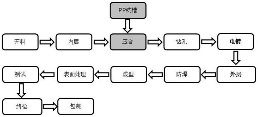
[0020] Such as image 3 As shown, a manufacturing method of a high-voltage circuit board includes: material cutting—inner layer manufacturing—press bonding—drilling—electroplating—outer layer manufacturing—solder masking—forming—surface treatment—testing—final inspection—packaging. In this embodiment, before pressing, at the designated position of the prepreg, a non-conductive slot is made by drilling or milling; then the prepreg with the slot, copper foil, and the inner layer The substrates are stacked in a given order (stacking according to the set order refers to stacking according to the design requirements of each PCB board to achieve the functions required by the design), and are pressed into a multi-layer circuit board in a high-temperature, high-pressure, vacuum environment. In a multilayer circuit board, the slot is located between two adjacent lines with a voltage difference on the substrate; the width of the slot is less than or equal to the distance between the two...
Embodiment 2
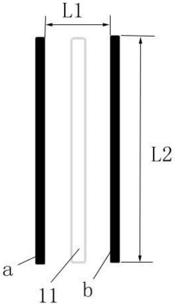
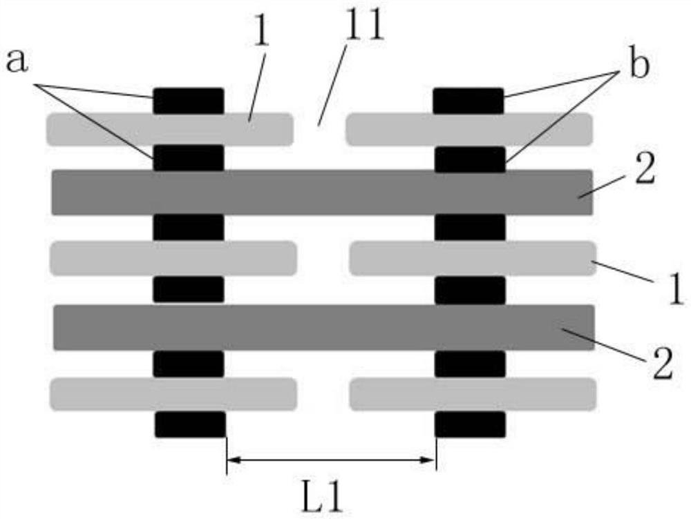
[0023] Based on the manufacturing method of the high-voltage circuit board described in Embodiment 1, this embodiment provides a high-voltage circuit board, and the high-voltage circuit board is manufactured by using the manufacturing method of the high-voltage circuit board described in Embodiment 1; figure 1 , figure 2 As shown, in the high-voltage circuit board, a slot 11 is made on the prepreg 1, and the slot 11 is located between two adjacent lines (line a, line b) with a voltage difference on the substrate 2; the slot The width of the hole 11 is less than or equal to the distance L1 between the two adjacent lines (line a, line b) with a voltage difference; the length of the slot is greater than or equal to the length of the parallel area of the two adjacent lines with a voltage difference L2; the substrate includes glass fiber cloth and insulating resin, and the glass fiber cloth is coated with silane as a coupling agent; the prepreg includes glass fiber cloth and ins...
PUM
 Abstract
Description
Claims
Application Information


