Array substrate, array substrate manufacturing method and display panel

An array substrate and substrate technology, applied in semiconductor/solid-state device manufacturing, instruments, electrical components, etc., and can solve problems such as complex processes and numerous film layers

Active Publication Date: 2021-09-07
WUHAN CHINA STAR OPTOELECTRONICS TECH CO LTD
View PDF8 Cites 1 Cited by
  • Summary
  • Abstract
  • Description
  • Claims
  • Application Information

AI Technical Summary

Problems solved by technology

The photosensitive semiconductor layer is set on the extension of the drain, which solves the problem that the cu...

Method used


Image

  • Array substrate, array substrate manufacturing method and display panel
  • Array substrate, array substrate manufacturing method and display panel
  • Array substrate, array substrate manufacturing method and display panel

Examples


Embodiment 1

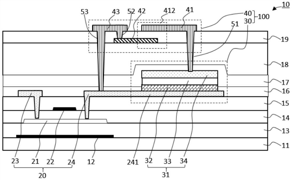
[0052] seefigure 1 , figure 1 It is a schematic diagram of the first structure of the array substrate provided in the embodiment of the present application. The array substrate 10 includes a base 11 , a thin film transistor 20 and a photosensor 100 . The thin film transistor 20 is arranged on the substrate 11, and the thin film transistor 20 includes a gate 22, an active layer 21, a source 23 and a drain 24 connected to the active layer 21; the photosensitive sensor 100 includes a photosensitive module 30 and a memory module 40, and the photosensitive module 30 includes a photosensitive semiconductor layer 31, and the memory module 40 includes a first electrode plate 41 and a second electrode plate 42; wherein, the photosensitive semiconductor layer 31 is arranged on the extension portion 241 of the drain, and the first electrode plate 41 is electrically connected to the photosensitive semiconductor layer 31 away from the side of the extension portion 241 of the drain 24 , the...

Embodiment 2

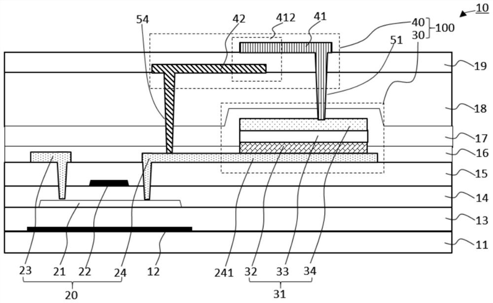
[0072] see figure 2 , figure 2 The second structure schematic diagram of the array substrate provided by the embodiment of the present application. The array substrate 10 of the embodiment of the present application is the same or similar to that of the first embodiment. The connection relation of the poles 24 is different.

[0073] The first insulating layer includes a fourth via hole 54 through which the second electrode plate 42 is connected to the drain electrode 24 .

[0074] specific, figure 2 The first insulating layer is the covering insulating layer 17 and the flat layer 18. In some cases, the array substrate 10 may only be provided with one of the covering insulating layer 17 and the flat layer 18. At this time, the first insulating layer is the covering insulating layer 17 and one of the flat layers 18.

[0075] In the embodiment of the present application, there is no connection electrode 43 in the first embodiment, and the second electrode plate 42 is direc...

Embodiment 3

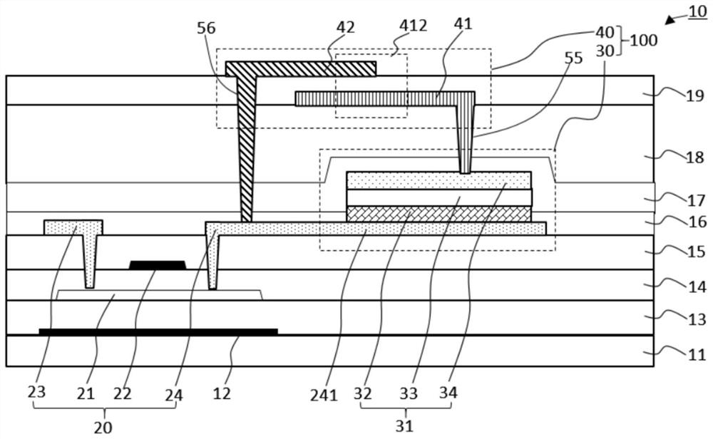
[0079] see image 3 , image 3 It is a schematic diagram of the third structure of the array substrate provided by the embodiment of the present application. The array substrate 10 of the embodiment of the present application is the same or similar to the first and second embodiments. The positional relationship between the plate 41 and the second electrode plate 42 is different.

[0080] In the embodiment of the present application, the first insulating layer is disposed on the photosensitive semiconductor layer 31 and the thin film transistor 20 , and the first electrode plate 41 is disposed on the first insulating layer.

[0081] specific, image 3 The first insulating layer is the covering insulating layer 17 and the planar layer 18. In some cases, the array substrate may only be provided with one of the covering insulating layer 17 and the planar layer 18. At this time, the first insulating layer is the covering insulating layer 17. and one of the planar layers 18 .

...


PUM


Abstract

The invention discloses an array substrate, an array substrate manufacturing method and a display panel. The array substrate comprises a substrate; a thin film transistor which is arranged on the substrate and comprises a grid electrode, an active layer, a source electrode and a drain electrode, wherein the source electrode and the drain electrode are connected with the active layer; and a photosensitive sensor which comprises a photosensitive module and a storage module, wherein the photosensitive module comprises a photosensitive semiconductor layer, and the storage module comprises a first electrode plate and a second electrode plate; wherein the photosensitive semiconductor layer is arranged on the extension part of the drain electrode, the first electrode plate is electrically connected with one side, far away from the extension part of the drain electrode, of the photosensitive semiconductor layer, and the second electrode plate is electrically connected with the drain electrode. The array substrate comprises the photosensitive sensor, the number of film layers of the photosensitive sensor is reduced, the number of manufacturing procedures of the array substrate can be reduced, and a photomask is saved.

Description

technical field [0001] The present application relates to the display field, and in particular to an array substrate, a method for manufacturing the array substrate, and a display panel. Background technique [0002] With the rapid development of the panel industry, in addition to the requirements for high resolution, wide viewing angle, and low power consumption of the display, people also put forward other requirements for the display panel. Enriching panel functions, increasing human-computer interaction, and improving the competitiveness of display panels are one of the main development directions of display panels at present. Integrating the ambient light sensor into the display panel can avoid punching holes in the screen or reducing the size of the screen due to the external ambient light sensor, and avoid affecting the appearance of the screen and the screen ratio. However, the current ambient light sensor integrated in the display panel has many film layers and com...

Claims


Application Information

Patent Timeline
IPC IPC(8): G09F9/30H01L27/32H01L21/77
CPCG09F9/30H10K59/13H01L27/1446H01L27/14692H01L27/1255H01L27/146H01L27/14609H01L27/1288
Inventor 龚帆艾飞宋继越
Owner WUHAN CHINA STAR OPTOELECTRONICS TECH CO LTD
Why Eureka
Try Eureka