Collimating device of optical sensor, and x-ray flat panel detector

An optical sensor and substrate technology, applied in the field of optical sensors, can solve the problems of complex preparation process of microlenses, difficulty in large-area production, and complicated procedures.

Pending Publication Date: 2021-09-10
TRULY SEMICON
View PDF0 Cites 0 Cited by
  • Summary
  • Abstract
  • Description
  • Claims
  • Application Information

AI Technical Summary

Problems solved by technology

The preparation process of microlenses is also very complicated. At present, photolithography, wet etching, nanoimprinting, etc. are mostly used, which require very precise molds to realize the preparation of microlenses.
The production of both collimators has disadvantages such as complicated procedures, high cost, difficulty in precise control, and difficulty in large-scale production.

Method used


Image

  • Collimating device of optical sensor, and x-ray flat panel detector
  • Collimating device of optical sensor, and x-ray flat panel detector
  • Collimating device of optical sensor, and x-ray flat panel detector

Examples


Embodiment 1

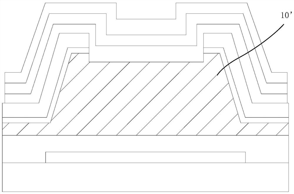
[0035] like Figure 4 Shown, an optical collimating device of the present invention provides a sensor comprising an optical sensor body 10; a first substrate 20 and second substrate 30, the first substrate 20 and second substrate 30 corresponding to the setting, the adhesive is made, easy to process, reduce production costs. Three black matrix, namely: a first black matrix 40, a second black matrix 41 and the third black matrix 42, the first black matrix 401 disposed on a first through hole 40, the second black matrix 41 provided on the second through hole 411, a third black matrix 421 is provided on the third through-hole 42. The first through hole 401, the center channel of the induction sensor and the optical center of the body 411 and the second through hole 421 coincides with the third through-hole. It plays a black matrix for shielding than the rest of the channel induced effects, effective control of the angle of incidence of light.

[0036] The black matrix structure of the...

Embodiment 2

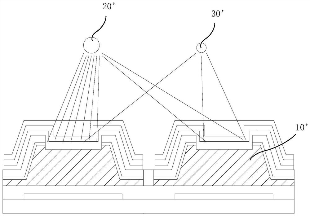
[0045] like Figure 5 with Image 6 As shown in Example 1 is different from, another configuration collimating means of the present embodiment provides an optical sensor, wherein the first substrate 20 and second substrate 30 stacked in the optical sensor 10 of a body side, the first substrate main body 20 close to the optical sensor 10 is provided.

[0046] Compared to the embodiment, the collimator device in Example 2 requires only two substrates, simplify processing steps, improve production efficiency, to save material.

[0047] Preferably, the thickness of the first substrate 20 is 0.1 0.2mm ~, thickness of the second substrate 30 is 0.4 ~ 0.7mm, the length of the channel of the photoreceptor 35 ~ 40μm, the length of the second through-hole 411 of the first through hole 401 ratio: 4: 7 to 5: 6, the second through hole 411 and the third through-hole 421 of the length ratio: 4: 7 to 5: 6.

Embodiment 3

[0049] The present invention also discloses a flat panel x-ray detector, such as Figure 7 Shown, optical sensors and collimation apparatus of Example 2 as an example, x-ray flat panel detector includes a scintillator 30 is connected to the second substrate 80, in order to avoid possible light source 81 is incident into the second through hole 411, a thickness of the second substrate 30 with the scintillator becomes required a large thickness body 80 becomes large; at the same time avoiding the third through hole 421 obliquely incident light enters the sensor, the thickness of the second substrate 30 to be considered a second the thickness and size of the through hole 411 of the first substrate 20. The thickness of the first substrate 20 as small as possible, to avoid oblique light intrusion sensor; a second substrate 30 as thick as possible. Preferably, the thickness of the first substrate 20 is 0.1 0.2mm ~, thickness of the second substrate 30 is 0.4 ~ 0.7mm, the length of the ch...


PUM

PropertyMeasurementUnit
thermal resistanceaaaaaaaaaa
optical densityaaaaaaaaaa

Abstract

The invention discloses a collimation device of an optical sensor, and an x-ray flat panel detector. The collimation device of the optical sensor comprises: a first substrate and a second substrate which are correspondingly arranged; and three the black matrixes including a first black matrix, a second black matrix and a third black matrix, wherein a first through hole is formed in the first black matrix, a second through hole is formed in the second black matrix, a third through hole is formed in the third black matrix, and the center of the first through hole, the center of the second through hole and the center of the third through hole coincide with the center of the sensing channel of the optical sensor body. The through holes in the black matrixes coincide with the center of the sensing channel of the optical sensor body, so the function of shading other parts is achieved, and the incident angle of light is effectively controlled; and the collimation device is formed by bonding the substrates in an aligned mode, so machining is convenient, and the manufacturing cost is reduced.

Description

Technical field [0001] Technical Field The present invention relates to optical sensors, and more particularly relates to an optical sensor apparatus and collimating x-ray flat panel detector. Background technique [0002] Optical sensors in industrial automation, industrial non-destructive testing, extensive artificial intelligence, medical diagnostics, consumer electronics and other fields of application. A thin film transistor-based optical sensors with low cost, large area imaging easy advantages. The typical structure constituting a basic pixel unit consists of a thin film transistor and a photosensitive member. In order to increase the photosensitive area, increase the filling ratio of the pixel, the thin film transistor is integrated with the photosensitive member, to make the π-type double gate structure, such as figure 1 Shown, both the amorphous silicon channel thin film transistor as an electron channel, is also used as a photosensitive, so-Si 10 'is a thickness of tho...

Claims


Application Information

Patent Timeline
Patent Type & Authority Applications(China)
IPC IPC(8): G01T1/20G01T1/202G01T7/00
CPCG01T1/20G01T1/2002G01T1/202G01T7/00
Inventor 罗志猛李源谢雄才
Owner TRULY SEMICON
Why Eureka
Try Eureka