Wiring layout adjustment method and device, electronic equipment and storage medium

A layout adjustment and routing technology, applied in the direction of electrical digital data processing, computer-aided design, special data processing applications, etc., can solve problems such as excessive human factors, slow efficiency, and low efficiency

Active Publication Date: 2021-09-10
ZHEJIANG UNIVIEW TECH CO LTD
View PDF9 Cites 0 Cited by
  • Summary
  • Abstract
  • Description
  • Claims
  • Application Information

AI Technical Summary

Problems solved by technology

However, the above-mentioned scheme has too many human factors, is prone to errors, and the adjustment speed is slow and inefficient.

Method used


Image

  • Wiring layout adjustment method and device, electronic equipment and storage medium
  • Wiring layout adjustment method and device, electronic equipment and storage medium
  • Wiring layout adjustment method and device, electronic equipment and storage medium

Examples


Embodiment 1

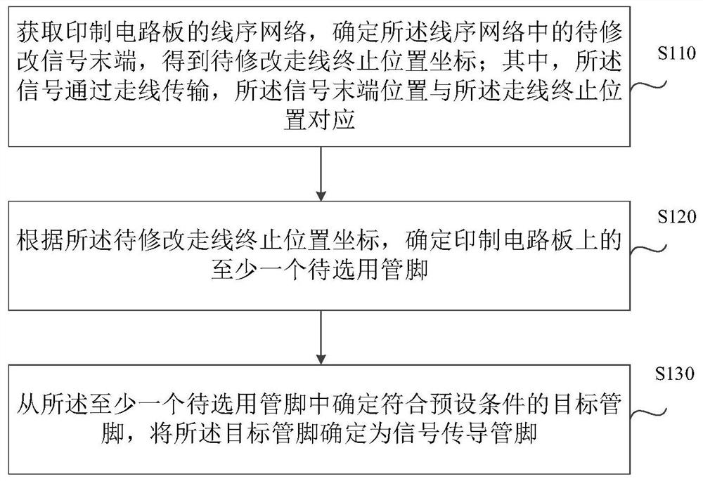
[0025] figure 1 It is a schematic flow chart of a routing layout adjustment method provided by Embodiment 1 of the present invention. This embodiment is applicable to the situation where it is difficult to get out of the PCB board during the design process. The method can be executed by a routing layout adjustment device. The device can be implemented in the form of software and / or hardware, and can be integrated into electronic equipment, specifically including the following steps:

[0026] Step 110: Obtain the line sequence network of the printed circuit board, determine the end of the signal to be modified in the line sequence network, and obtain the coordinates of the termination position of the line to be modified; wherein, the signal is transmitted through the line, and the position of the signal end is Corresponding to the termination position of the trace.

[0027] In this embodiment, a printed circuit board, also called a printed circuit board, is a platform for elec...

Embodiment 2

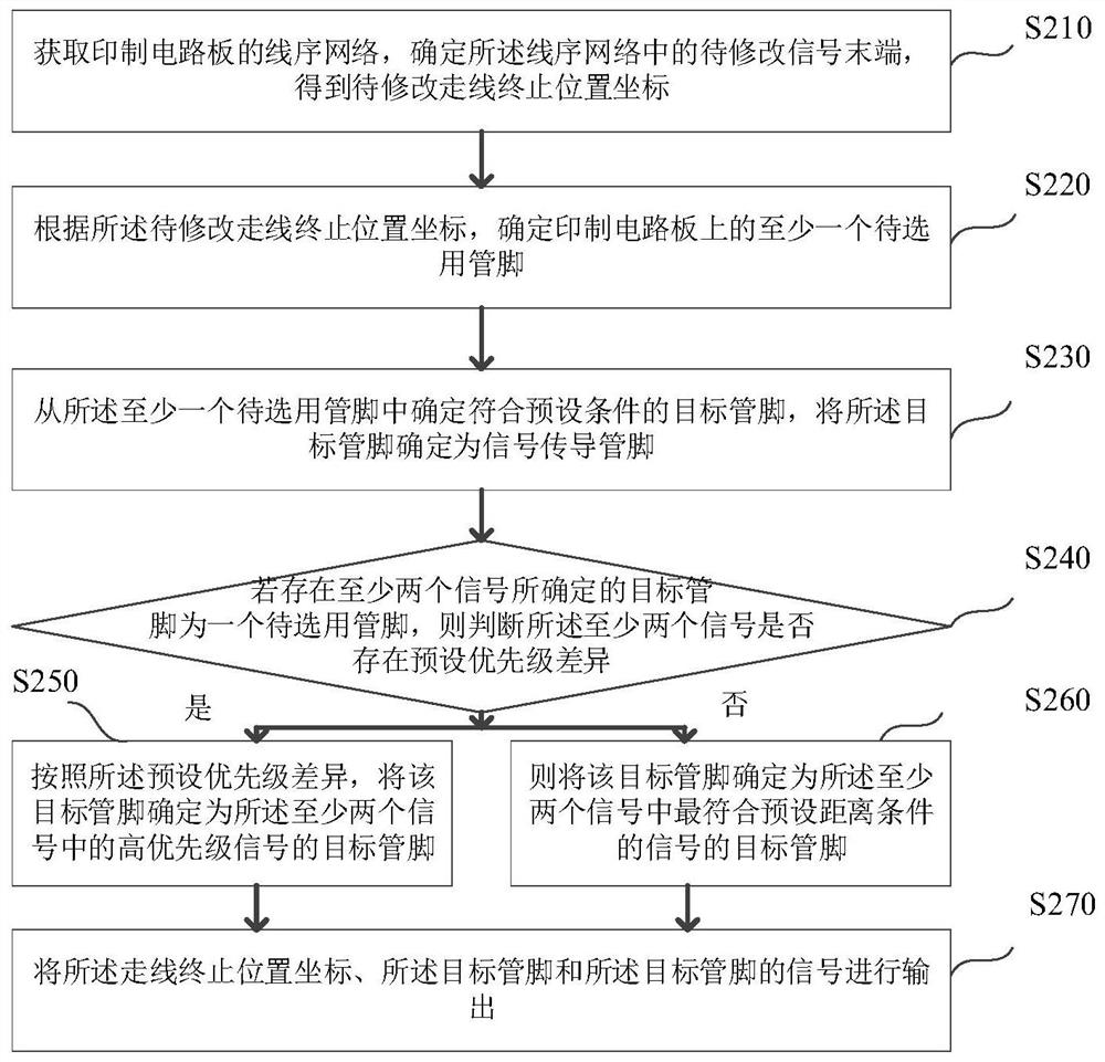
[0043] figure 2 It is a schematic flow chart of a routing layout adjustment method provided by Embodiment 2 of the present invention. This embodiment is further optimized on the basis of the above embodiments. The specific optimization is: how to further determine the target pin, specifically as follows step:

[0044] Step 210: Obtain the line sequence network of the printed circuit board, determine the end of the signal to be modified in the line sequence network, and obtain the coordinates of the termination position of the line to be modified.

[0045] Wherein, the signal is transmitted through a wire, and the end position of the signal corresponds to the end position of the wire.

[0046] Step 220: Determine at least one pin to be selected on the printed circuit board according to the coordinates of the termination position of the trace to be modified.

[0047] Step 230: Determine a target pin that meets a preset condition from the at least one candidate pin, and determ...

Embodiment 3

[0060] Figure 4 It is a schematic structural diagram of a wiring layout adjustment device provided in Embodiment 3 of the present invention. A wiring layout adjusting device provided in an embodiment of the present invention can execute a wiring layout adjusting method provided in any embodiment of the present invention, and has corresponding functional modules and beneficial effects for executing the method. Such as Figure 4 As shown, the device includes:

[0061] The coordinate determination module 401 of the termination position of the trace is used to obtain the line sequence network of the printed circuit board, determine the end of the signal to be modified in the line sequence network, and obtain the coordinates of the termination position of the trace to be modified; wherein, the signal passes through the trace line transmission, the position of the end of the signal corresponds to the termination position of the wiring;

[0062] A pin to be selected determining m...


PUM


Abstract

The invention discloses a routing layout adjustment method and device, electronic equipment and a storage medium. The method comprises the following steps: collecting a line sequence network of the printed circuit board, determining a to-be-modified signal tail end in the line sequence network, and obtaining a to-be-modified wiring termination position coordinate; wherein the signal is transmitted through a wire, and the tail end position of the signal corresponds to the end position of the wire; determining at least one pin to be selected on the printed circuit board according to the termination position coordinates of the wiring to be modified; and determining a target pin meeting a preset condition from the at least one to-be-selected pin, and determining the target pin as a signal conduction pin. By adopting the technical scheme, the pin signal can be more efficiently and accurately adjusted when the line outgoing of the printed circuit board is difficult.

Description

technical field [0001] The invention relates to the technology of the electronic industry, in particular to a wiring layout adjustment method, device, electronic equipment and storage medium. Background technique [0002] PCB (Printed circuit boards, printed circuit boards) is one of the important components of the electronics industry, and almost every electronic device uses PCBs. From small electronic watches and calculators to large computers, communication electronic equipment, military weapon systems, etc. [0003] In complex PCB design, it is often found in the layout or wiring stage that the wiring sequence of some parts of the chip is not in order, which makes it difficult to get out of the wiring. At this time, the following methods will be used to solve the problem: punching holes to force the layer to go out; adjusting the layout of the chip or interface to straighten out the line; checking the chip information and adjusting the signal definition. However, the a...

Claims


Application Information

Patent Timeline
Patent Type & Authority Applications(China)
IPC IPC(8): G06F30/392
Inventor 虞程华张立辉陈欢洋
Owner ZHEJIANG UNIVIEW TECH CO LTD
Why Eureka
Try Eureka