Optoelectronic semiconductor device

An optoelectronic semiconductor and semiconductor technology, applied in the field of optoelectronics, can solve the problems affecting the stability of optoelectronic semiconductor devices, inflow, short circuit of optoelectronic semiconductor devices, etc.

Inactive Publication Date: 2021-09-10
粟安海
View PDF0 Cites 0 Cited by
  • Summary
  • Abstract
  • Description
  • Claims
  • Application Information

AI Technical Summary

Problems solved by technology

[0003] When using optoelectronic semiconductor devices, it is necessary to package the optoelectronic semiconductor devices. During the packaging process, since the pins need to be led out, the interface of the general pins will be larger than the area of ​​the pins, so that there will be a certain amount of direct contact between the pins and the interface. The gap between the t

Method used


Image

  • Optoelectronic semiconductor device
  • Optoelectronic semiconductor device
  • Optoelectronic semiconductor device

Examples


Embodiment 1

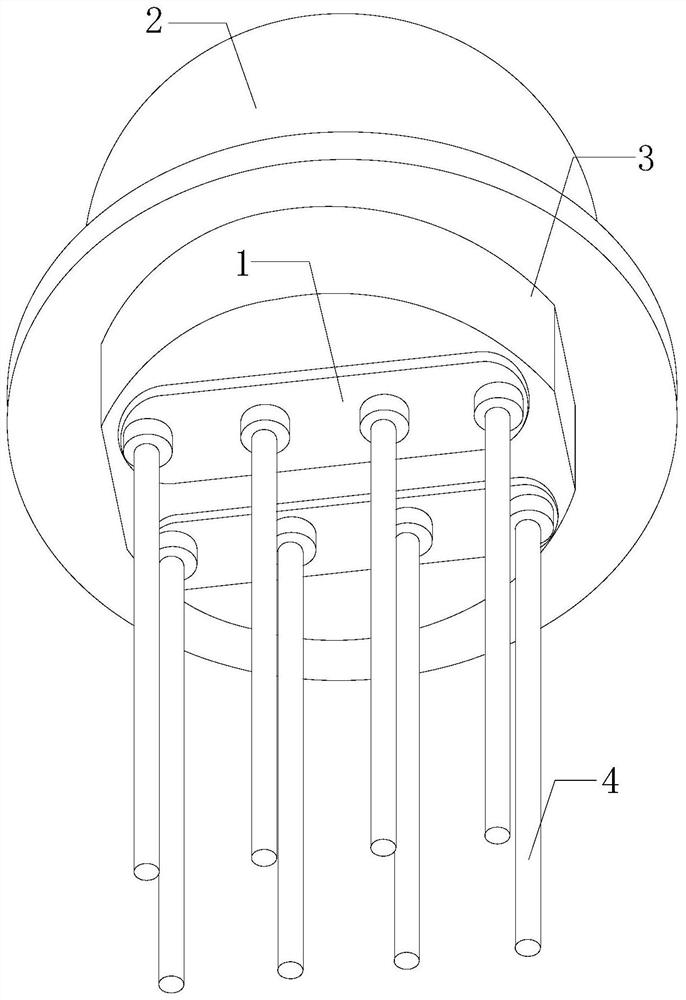
[0029] See figure 1 The present invention provides a technical solution: An optoelectronic semiconductor device, the structure comprising a quench apparatus 1, the enclosure 2, the semiconductor device 3, the pin 4, the sealing device 1 is provided with two barrier, two quench apparatus 1 is mounted on the enclosure 2, the enclosure 2 is provided inside the semiconductor device 3, the semiconductor device 3 is integral with the pin 4, the pin 42 and the through-quench means connected to the enclosure 1 .

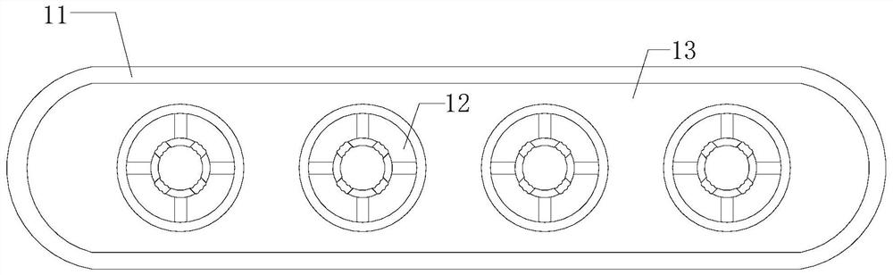
[0030] See figure 2 , The sealing means comprises a barrier frame 11, the barrier assembly 12, the connecting plate 13, the frame body 11 and the connecting plate 13 engaged with sleeve, the connecting plate 12 is provided with four barrier assembly 13, four barrier assembly 12 equidistantly arranged on the transverse web 13, the housing 11 is mounted on the enclosure 2, the barrier assembly 12 is connected to pin 4.

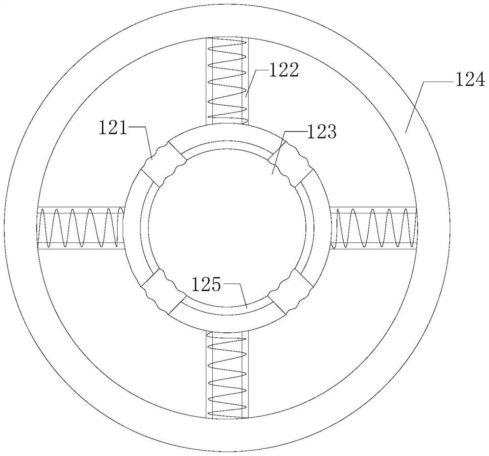
[0031] See image 3 The barrier assembly 12 includes a tensio...

Embodiment 2

[0041] See figure 1 The present invention provides a technical solution: an optoelectronic semiconductor device comprising a barrier device 1, a package cavity 2, a semiconductor device 3, a pin 4, and the blocking device 1 is provided with two, two blocking The device 1 is mounted on the encapsulation chamber 2, and the inner portion of the package chamber 2 is provided with a semiconductor device 3 and the pin 4, and the tube foot 4 is connected to the blocking device 1. .

[0042] See figure 2 The barrier device 1 includes a casing 11, a barrier assembly 12, a connecting plate 13, and the casing 11 is associated with the connecting plate 13, and the connecting plate 13 is provided with four barrier assemblies 12, four The barrier assembly 12 is equivalent to the lateral laterally arranged on the connecting plate 13, the housing 11 being mounted on the encapsulation chamber 2, the barrier assembly 12 to the pin 4.

[0043] See image 3 The barrier assembly 12 includes a tension m...


PUM


Abstract

The invention discloses an optoelectronic semiconductor device, which structurally comprises a blocking and sealing device, a packaging cavity, a semiconductor device body and a pin. According to the invention, when the optoelectronic semiconductor device is used, a worker manually opens four attaching blocking pieces outwards, a tension piece is opened accordingly, a pin vertically and downwards extends into an interface, the worker slowly loosens the attaching blocking pieces, an elastic rod can generate resilience force under the condition that the elastic rod is not stressed, the attaching blocking pieces can be pushed inwards under the resilience inertia of the elastic rod, the four attaching blocking pieces can retract inwards at the same time to be attached to the pin, the tension piece can also be attached to the side wall of the pin along with retraction of the attaching blocking pieces, and air outside the pin is blocked through mutual cooperation of the attaching blocking pieces and the tension piece, so that the use stability of the optoelectronic semiconductor device is ensured.

Description

Technical field [0001] The present invention relates to the field of optoelectronics, particularly relates to an optoelectronic semiconductor device. Background technique [0002] With the rapid development of information technology, the optoelectronic semiconductor device is widely used, the design principle of the optoelectronic semiconductor device is based on the external field changes the propagation mode of the guided light, the optoelectronic semiconductor device is broadly divided into two categories: one is the electrical energy into light energy a light emitting device; one is the light energy into electrical energy photosensitive component, a barrier for blocking the outside air through the element, during use of the optoelectronic semiconductor devices, for improvement: [0003] During use of the optoelectronic semiconductor component, the optoelectronic semiconductor device needs to be packaged, during the packaging process, due to the need for lead-out pin, generall...

Claims


Application Information

Patent Timeline
IPC IPC(8): H01L31/0203H01L31/00
CPCH01L31/0203H01L31/00
Inventor 粟安海
Owner 粟安海
Why Eureka
Try Eureka