Pseudo resistance circuit and cascade circuit thereof

A cascaded circuit, pseudo-resistor technology, applied in the network of analog resistance, improvement of network to reduce the influence of temperature change, single-port active network, etc.

Active Publication Date: 2021-09-10
上海料聚微电子有限公司
View PDF6 Cites 0 Cited by
  • Summary
  • Abstract
  • Description
  • Claims
  • Application Information

AI Technical Summary

Problems solved by technology

[0003] There are still some problems with pseudo-resistors implemented by such as MOS transistors

Method used


Image

  • Pseudo resistance circuit and cascade circuit thereof
  • Pseudo resistance circuit and cascade circuit thereof
  • Pseudo resistance circuit and cascade circuit thereof

Examples


Embodiment Construction

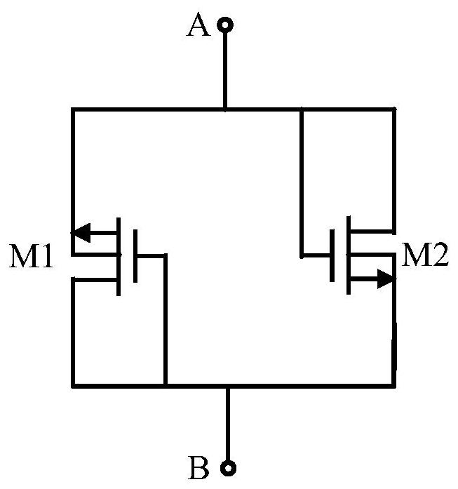
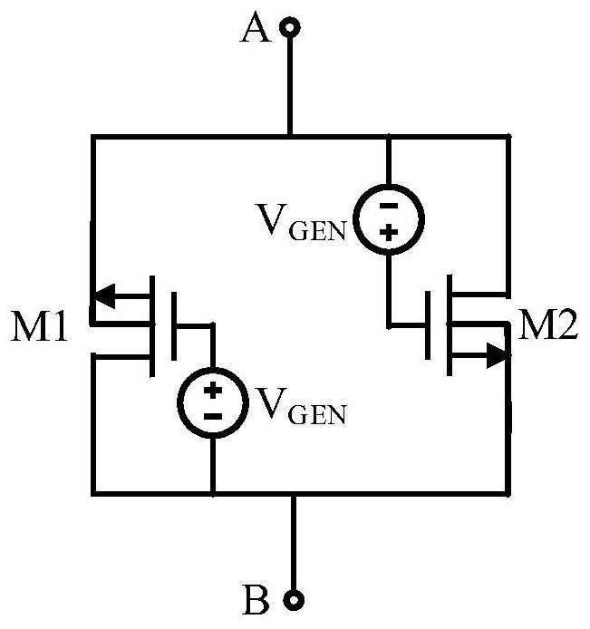
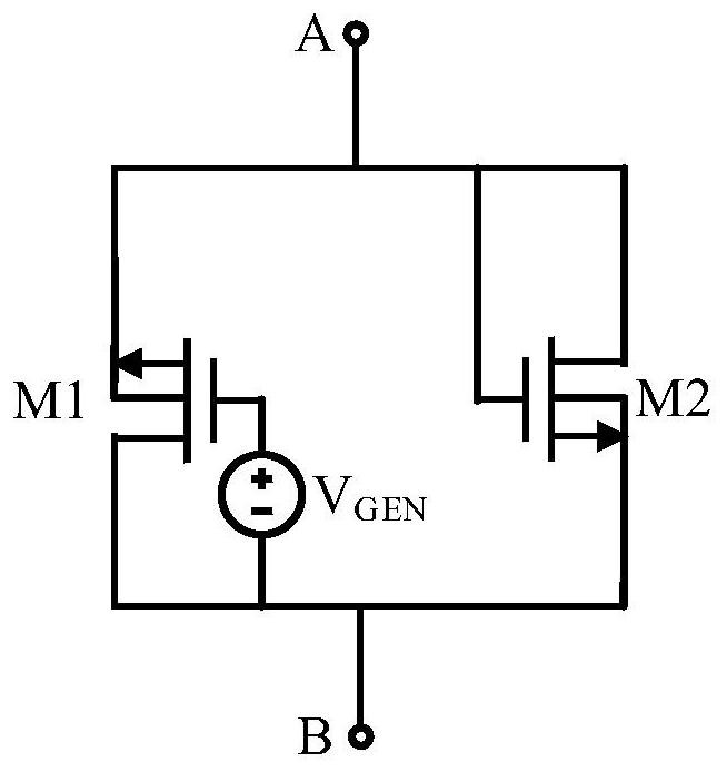
[0052] The present invention will be further described in detail below through specific embodiments in conjunction with the accompanying drawings. Wherein, similar elements in different implementations adopt associated similar element numbers. In the following implementation manners, many details are described for better understanding of the present application. However, those skilled in the art can readily recognize that some of the features can be omitted in different situations, or can be replaced by other elements, materials, and methods. In some cases, some operations related to the application are not shown or described in the description, this is to avoid the core part of the application being overwhelmed by too many descriptions, and for those skilled in the art, it is necessary to describe these operations in detail Relevant operations are not necessary, and they can fully understand the relevant operations according to the description in the specification and genera...


PUM


Abstract

The invention discloses a pseudo resistance circuit and a cascade circuit thereof, and the pseudo resistance circuit comprises: a transistor M1 which is provided with a first electrode, a second electrode and a control electrode, wherein the first electrode and the second electrode of the transistor M1 are respectively connected with the second end and the first end; a bias voltage generating circuit which corresponds to the transistor M1, wherein two ends of the bias voltage generating circuit are respectively connected with the first electrode and the control electrode of the transistor M1, and the bias voltage generating circuit is used for increasing the bias voltage between the first electrode and the control electrode of the transistor M1; and a transistor M2 which is provided with a first electrode, a second electrode and a control electrode, wherein the first electrode and the second electrode of the transistor M2 are connected with the first end and the second end respectively, and the first electrode of the transistor M2 is further connected with the control electrode of the transistor M2. According to the invention, the bias voltage generation circuit VGEN is used to solve some problems of a current pseudo resistor, such as the improvement of the linearity of an equivalent resistance value and the like.

Description

technical field [0001] The invention relates to the field of integrated circuits, in particular to a pseudo-resistance circuit and a cascaded circuit thereof. Background technique [0002] When making a resistor with an ultra-large resistance value (generally GΩ level) under such as MOS process conditions, it needs to occupy a very large area. Therefore, in order to reduce the chip area required to realize the ultra-large resistance, the inventors of those skilled in the art use such as MOS transistors To realize a pseudo-resistor with a large resistance value, thereby replacing the traditional resistor. [0003] There are still some problems with pseudo-resistors implemented by, for example, MOS transistors. Contents of the invention [0004] The present invention proposes a pseudo-resistance circuit and its cascaded circuit, which will be described in detail below. [0005] According to the first aspect, a pseudo-resistance circuit is provided in an embodiment, includi...

Claims


Application Information

Patent Timeline
Patent Type & Authority Applications(China)
IPC IPC(8): H03H11/46H03H11/54
CPCH03H11/53H03H11/54Y02D10/00
Inventor 李小勇李威
Owner 上海料聚微电子有限公司
Why Eureka
Try Eureka