

Skin conductivity measuring method and device and wearable equipment
A skin conductivity and measurement method technology, applied in the field of wearable devices, can solve the problems of high equipment cost, incomplete conductance data range measurement, and the inability of a single ADC chip to completely cover the measurement signal, etc.
- Summary
- Abstract
- Description
- Claims
- Application Information
AI Technical Summary
Problems solved by technology
Method used
Image

Examples
Embodiment Construction
[0027] Exemplary embodiments of the present application will be described in more detail below with reference to the accompanying drawings. Although exemplary embodiments of the present application are shown in the drawings, it should be understood that the present application may be embodied in various forms and should not be limited to the embodiments set forth herein. Rather, these embodiments are provided so that the present application can be more thoroughly understood, and the scope of the present application can be fully conveyed to those skilled in the art.
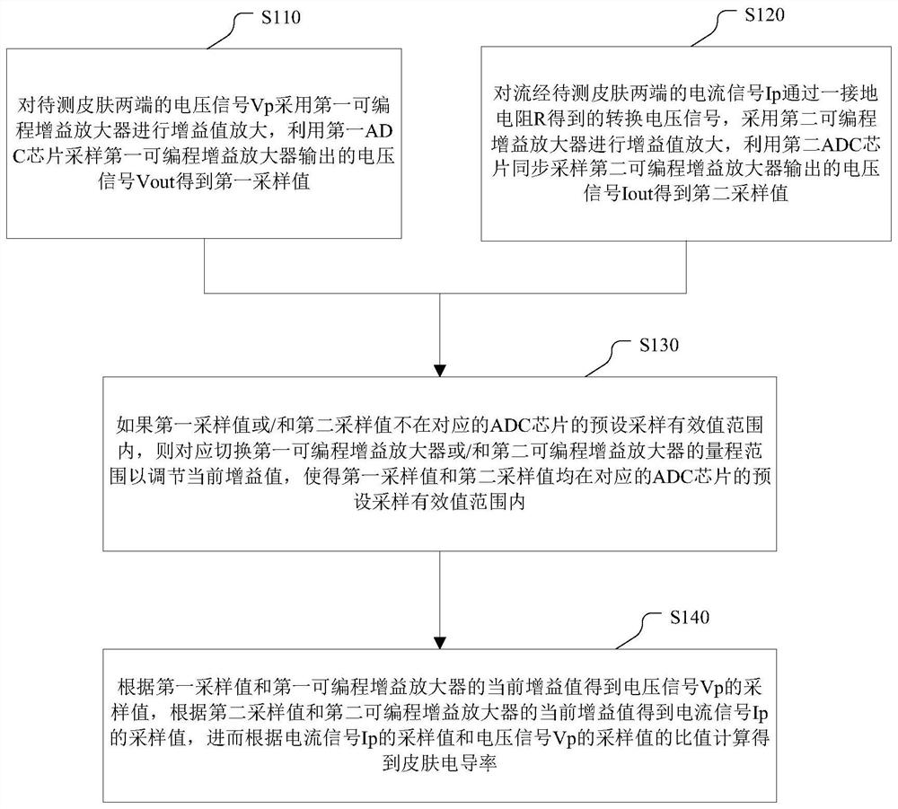
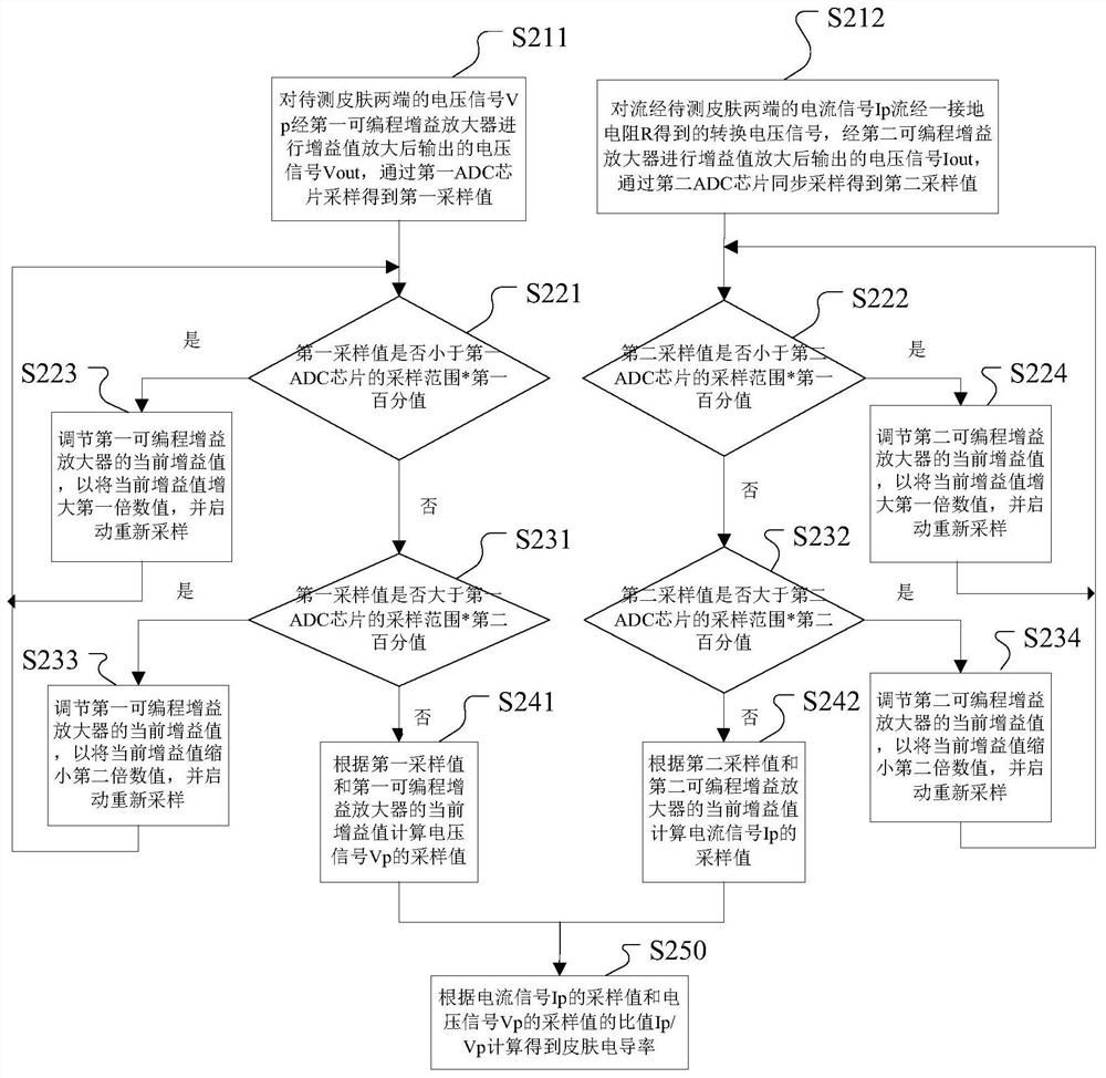
[0028] figure 1 A schematic flowchart of a method for measuring skin conductivity according to an embodiment of the present application is shown. Such as figure 1 As shown, the method includes:
[0029] In step S110, the voltage signal Vp at both ends of the skin to be tested is amplified by the first programmable gain amplifier, and the first ADC chip is used to sample the voltage signal Vout output by the fir...
PUM
 Abstract
Description
Claims
Application Information