Array substrate, manufacturing method and display panel

A technology of an array substrate and a manufacturing method, which can be applied to instruments, nonlinear optics, optics, etc., and can solve problems such as depolarization of display panels

Active Publication Date: 2021-09-14
KUSN INFOVISION OPTOELECTRONICS
View PDF6 Cites 1 Cited by
  • Summary
  • Abstract
  • Description
  • Claims
  • Application Information

AI Technical Summary

Problems solved by technology

[0006] In order to overcome the shortcomings and deficiencies existing in the prior art, the object of the present invention is to provide an array substrate, a manufacturing method, and a display panel to solve the problem of depolarization in the display panel in the prior art

Method used


Image

  • Array substrate, manufacturing method and display panel
  • Array substrate, manufacturing method and display panel
  • Array substrate, manufacturing method and display panel

Examples


Embodiment 1

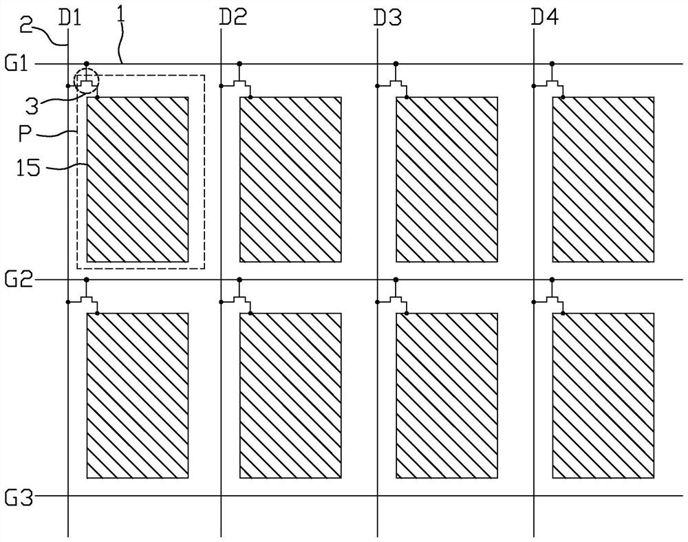
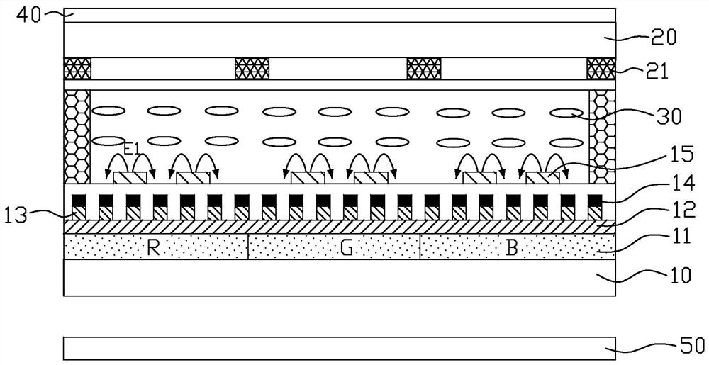
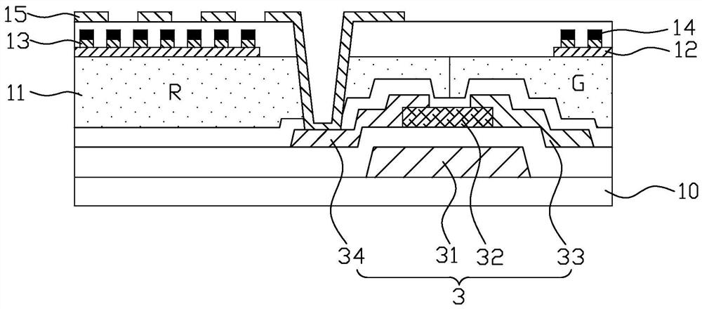
[0059] figure 1 is a schematic plan view of the array substrate in the present invention, figure 2 is a schematic cross-sectional structure diagram of the display panel in Embodiment 1 of the present invention, image 3 is a schematic cross-sectional view of the array substrate at the thin film transistor in Embodiment 1 of the present invention.

[0060] Such as Figure 1 to Figure 3 As shown, an array substrate provided by Embodiment 1 of the present invention includes a substrate 10 and scan lines 1 , data lines 2 , thin film transistors 3 and pixel electrodes 15 disposed on the substrate 10 . A plurality of pixel units P are formed on the substrate 10 by a plurality of scanning lines 1 and a plurality of data lines 2 insulated from each other and intersecting each other. Each pixel unit P is provided with a thin film transistor 3 and a pixel electrode 15, and each pixel electrode 15 passes through an adjacent pixel. The thin film transistor 3 of the electrode 15 is ele...

Embodiment 2

[0084] Figure 5 is a schematic cross-sectional view of the array substrate at the thin film transistor in Embodiment 2 of the present invention. Such as Figure 5 As shown, the array substrate, the manufacturing method and the display panel provided by Embodiment 2 of the present invention are the same as Embodiment 1 ( figure 1 The array substrate and the manufacturing method in FIG. 4) are basically the same as the display panel, except that, in this embodiment, the pixel electrode 15 is arranged on the surface of the quantum dot layer 11 away from the substrate 10 and is connected to the quantum dot layer. The layer 11 is in direct contact, the metal wire grid polarizer 13 is arranged on the side surface of the pixel electrode 15 away from the substrate 10 and is in direct contact with the pixel electrode 15, and the common electrode 12 is arranged on the side of the metal wire grid polarizer 13 away from the pixel electrode 15 . That is, in this embodiment, the common ...

Embodiment 3

[0101] Image 6 is a schematic cross-sectional structure diagram of the display panel in Embodiment 3 of the present invention, Figure 7 is a schematic cross-sectional view of the array substrate at the thin film transistor in Embodiment 3 of the present invention, Figures 8a-8f It is a schematic diagram of the manufacturing process of the manufacturing method of the array substrate in the third embodiment of the present invention. Such as Image 6 - As shown in FIG. 8, the array substrate, the manufacturing method and the display panel provided by Embodiment 3 of the present invention are the same as Embodiment 1 ( figure 1 The array substrate and the manufacturing method in FIG. 4) are basically the same as the display panel. The difference is that, in this embodiment, the quantum dot layer 11 is arranged on the surface of the substrate 10 and is in direct contact with the substrate 10. The scanning lines 1, The data line 2 and the thin film transistor 3 are disposed on a...


PUM

PropertyMeasurementUnit
diameteraaaaaaaaaa

Abstract

The invention discloses an array substrate, a manufacturing method and a display panel. The array substrate comprises a substrate, and scanning lines, data lines, thin film transistors, a quantum dot layer, a metal wire grid polaroid, an anti-reflection layer and pixel electrodes which are arranged on the substrate, wherein each pixel electrode is electrically connected with the corresponding scanning line and data line through the thin film transistor, the metal wire grid polaroid is arranged on the side, away from the substrate, of the quantum dot layer, the anti-reflection layer is arranged on the side, away from the quantum dot layer, of the metal wire grid polaroid, the metal wire grid polaroid comprises a plurality of metal wires which are parallel to one another and arranged at intervals, the anti-reflection layer comprises a plurality of light absorption wires which are parallel to one another and arranged at intervals, and the light absorption wires are in one-to-one correspondence with the metal wires. According to the invention, the metal wire grid polaroid is arranged on the side, away from the substrate, of the quantum dot layer and matched with the anti-reflection layer corresponding to the metal wire grid polaroid, so that the color gamut is improved while the problems of depolarization and ambient light reflection can be prevented so as to improve the contrast ratio.

Description

technical field [0001] The invention relates to the technical field of displays, in particular to an array substrate, a manufacturing method, and a display panel. Background technique [0002] With the development of display technology, thinner and lighter display panels are favored by consumers, especially thinner and lighter display panels (liquid crystal display, LCD). [0003] An existing display panel includes a thin film transistor array substrate (Thin Film Transistor Array Substrate, TFT Array Substrate), a color filter substrate (Color Filter Substrate, CF Substrate), and a liquid crystal filled between the thin film transistor array substrate and the color filter substrate. Molecules, when the above-mentioned display panel is working, a driving voltage is applied to the thin-film transistor array substrate and the color filter substrate respectively, and the rotation direction of the liquid crystal molecules between the two substrates is controlled to refract the b...

Claims


Application Information

Patent Timeline
Patent Type & Authority Applications(China)
IPC IPC(8): G02F1/13357G02F1/1335G02F1/1343G02F1/1362G02F1/1368
CPCG02F1/133614G02F1/13362G02F1/133605G02F1/136286G02F1/1368G02F1/134309G02F2201/121G02F2201/123
Inventor 钟德镇沈家军姜丽梅
Owner KUSN INFOVISION OPTOELECTRONICS
Why Eureka
Try Eureka