Pressing structure of PCB and processing method of PCB

A PCB board and processing method technology, applied in the field of PCB processing, can solve problems affecting the normal use of electronic products, board surface warpage, etc., to achieve the effect of reducing warpage and maintaining pressing efficiency

Active Publication Date: 2021-09-21
KALEX MULTI LAYER CIRCUIT BOARD (ZHONGSHAN) CO LTD
View PDF4 Cites 0 Cited by
  • Summary
  • Abstract
  • Description
  • Claims
  • Application Information

AI Technical Summary

Problems solved by technology

For asymmetric PCB boards, the use of traditional lamination methods is prone to board warpage, which will adversely affect the preparation, assembly, and signal transmission of PCB boards, thereby affecting the normal use of electronic products

Method used


Image

  • Pressing structure of PCB and processing method of PCB
  • Pressing structure of PCB and processing method of PCB
  • Pressing structure of PCB and processing method of PCB

Examples


Embodiment 1

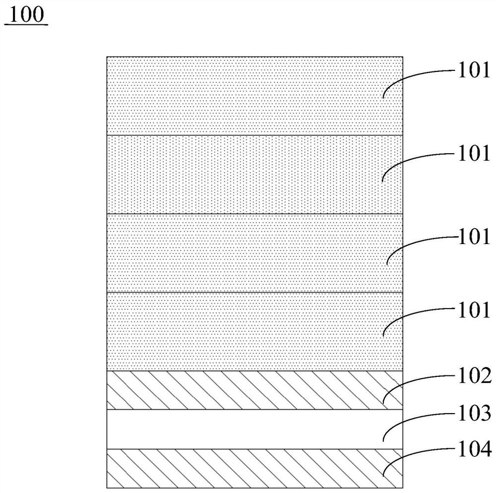
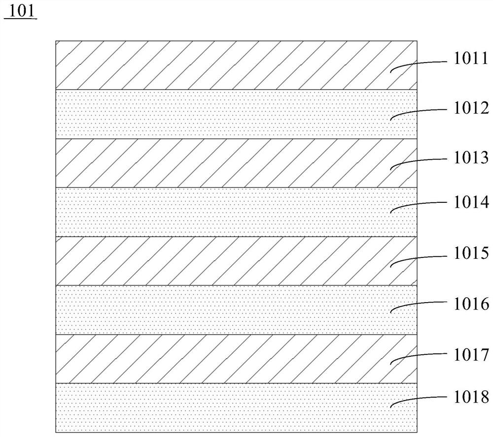
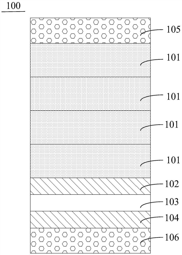
[0069] In this embodiment, the pressing structure is as image 3 As shown, where the row of board layers is as figure 2 As shown, there are 4 board layers. The direction of the BOT surface of the core layer of the 1st to 2nd rowing layers is opposite to the direction of the BOT surface of the core layer of the 3rd to 4th rowing layer. That is to say, the BOT face of the core layer of the 1st to 2nd row of board layers faces down, and the BOT face of the core layer of the 3rd to 4th row of board layers faces up.

[0070] The first buffer layer, the second buffer layer, the first prepreg layer and the second prepreg layer are all prepreg layers formed of prepreg sheets.

[0071] The first isolation layer, the second isolation layer, the third isolation layer and the fourth isolation layer are copper foil layers with a thickness of 0.5 oz.

[0072] The thickness of the first copper foil layer is 0.5 oz, and the thickness of the second copper foil layer is 0.5 oz. The thickne...


PUM


Abstract

The invention relates to a pressing structure of a PCB and a processing method of the PCB. In the pressing structure, through the arrangement of a first isolation layer, a second isolation layer, a third isolation layer, a fourth isolation layer, a first buffer layer and a second buffer layer, the influence of instantaneous high temperature and high pressure on a first copper foil layer, a first semi-cured layer, a core board layer, a second semi-cured layer and a second copper foil layer during pressing can be effectively avoided, and the flatness of the first copper foil layer, the core board layer and the second copper foil layer is kept. Furthermore, the even number of board arrangement layers are sequentially stacked, and the BOT surfaces of the core board layers of the first to nth board arrangement layers are opposite to the BOT surfaces of the core board layers of the (n+1)-2nth board arrangement layers in orientation, so that the internal stress of the pressing structure in the pressing process can be effectively balanced, and the flatness of the first copper foil layer, the core board layers and the second copper foil layer can be better maintained; and the PCB is further prevented from warping after being laminated.

Description

technical field [0001] The invention relates to the field of PCB processing, in particular to a pressing structure of a PCB board and a processing method of the PCB board. Background technique [0002] With the continuous upgrading of electronic products, there are more and more products with high-speed signal transmission. For example, the current popular 5G products have an increasing market share. In the manufacturing components of electronic products, as a basic component, the design of PCB is becoming more and more complicated. In complex PCB design, there are more and more asymmetric PCBs, such as inconsistent copper thickness of the inner core board, or inconsistent copper thickness of core boards of different layers. For asymmetric PCB boards, the use of traditional lamination methods is prone to board warpage, which will adversely affect the preparation, assembly, and signal transmission of PCB boards, thereby affecting the normal use of electronic products. Cont...

Claims


Application Information

Patent Timeline
Patent Type & Authority Applications(China)
IPC IPC(8): H05K3/46H05K3/00
CPCH05K3/4644H05K3/0097
Inventor 李鸿辉曹振兴
Owner KALEX MULTI LAYER CIRCUIT BOARD (ZHONGSHAN) CO LTD
Why Eureka
Try Eureka