Packaging mechanism and packaging method for semiconductor substrate

A packaging method and semiconductor technology, applied in the direction of semiconductor devices, semiconductor/solid-state device manufacturing, semiconductor/solid-state device components, etc., can solve the problems of relaxation, the substrate cannot be adjusted, the semiconductor substrate is loose, etc., and achieves high assembly convenience. Effect

Active Publication Date: 2021-09-28
山东普利斯林智能仪表有限公司
View PDF18 Cites 2 Cited by
  • Summary
  • Abstract
  • Description
  • Claims
  • Application Information

AI Technical Summary

Problems solved by technology

[0005] In order to solve the above-mentioned technical problems, the present invention provides a packaging mechanism and packaging method for semiconductor substrates to solve the gap between the packaging structure and the internal semiconductor components, chips, and substrates during the packaging process of the semiconductor substrate in the prior art. It cannot be adjusted, and the sealing components tightly connected to the semiconductor substrate will deform and loosen as the usage time increases. There is no tightness adjustment structure inside the packaging structure, and the semiconductor substrate that is tightly packaged will become loose with the extension of usage time.

Method used


Image

  • Packaging mechanism and packaging method for semiconductor substrate
  • Packaging mechanism and packaging method for semiconductor substrate
  • Packaging mechanism and packaging method for semiconductor substrate

Examples


Embodiment

[0034] as attached figure 1 to attach Figure 10 Shown:

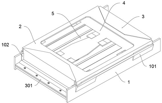
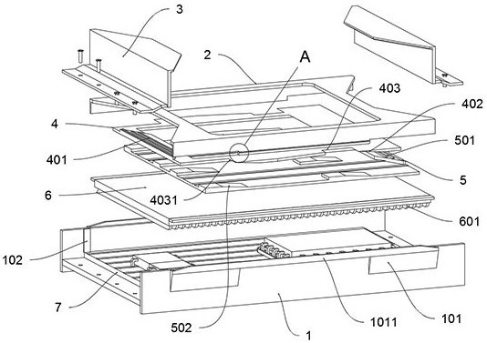
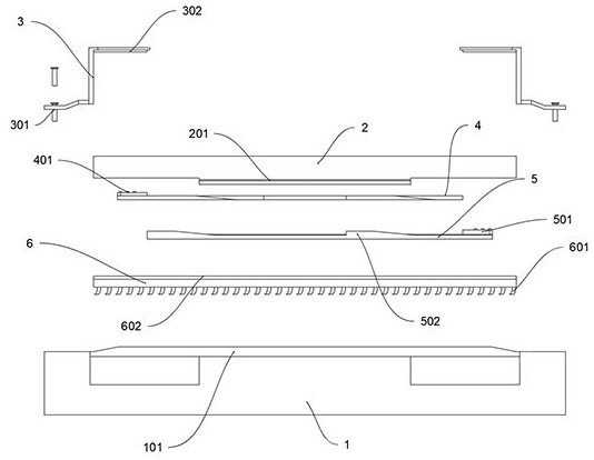
[0035]The present invention provides a packaging mechanism and packaging method for semiconductor substrates, including a packaging base 1; a semiconductor electrical substrate 7 is fixedly connected in the middle of the packaging base 1; above the body; the side packaging module 3 is provided with two groups, and the two groups are respectively located on the left side and the right side of the upper cover plate 2, and the bottom of the side packaging module 3 is fixedly connected to the upper surface of the bottom plate of the packaging seat 1 by screws; the upper clamping interlayer 4 It is located on the lower surface of the upper cover plate 2, and there is also a lower tightening interlayer 5 below the upper tightening interlayer 4, and the upper tightening interlayer 4 and the lower tightening interlayer 5 are all movably connected inside the upper cover plate 2; Both ends are connected to the two side walls of...


PUM


Abstract

The invention provides a packaging mechanism and a packaging method for a semiconductor substrate, belongs to the technical field of semiconductor substrate packaging structures, and aims to solve the problems that in the packaging process of the semiconductor substrate in the prior art, the packaging structure cannot be adjusted with internal semiconductor components, chips and substrates, a sealing assembly which is tightly connected with a semiconductor substrate deforms and loosens along with the prolonging of the service time, the interior of a packaging structure is lack of a tightness adjusting structure, and the tightly packaged semiconductor substrate loosens along with the prolonging of the service time. The packaging mechanism comprises a packaging seat; a semiconductor electrical substrate is fixedly connected to the middle of the interior of the packaging seat, and the packaging seat comprises a side wall positioning frame; the two ends of a buffer pressing layer are connected to the two side walls of the packaging base through gluing. A substrate and a base can be prevented from being loose in connection during long-term use, simple reinforcement can be performed, and the connection tightness between the semiconductor substrate and the base can be maintained.

Description

technical field [0001] The invention belongs to the technical field of semiconductor substrate packaging structures, and more specifically relates to a packaging mechanism and packaging method for semiconductor substrates. Background technique [0002] The package substrate is an important part of the electronic package, and it is the bridge between the chip and the external circuit. In the package, the substrate plays the role of realizing the transmission of current and signal between the chip and the outside world, mechanically protecting and supporting the chip, dissipating heat from the chip to the outside world, and transitioning the space between the chip and the external circuit. The substrate material is used to manufacture semiconductor components. And the basic material of printed circuit board. [0003] For example, the application number: CN201610132896.8 The present invention discloses an electronic package and its semiconductor substrate and manufacturing met...

Claims


Application Information

Patent Timeline
Patent Type & Authority Applications(China)
IPC IPC(8): H01L23/04H01L23/10H01L23/13H01L23/16H01L21/50H01L21/52
CPCH01L23/04H01L23/10H01L23/13H01L23/16H01L21/50H01L21/52
Inventor 陈冬岩都洪涛黄晓雷
Owner 山东普利斯林智能仪表有限公司
Why Eureka
Try Eureka