Matcher output power debugging method and debugging system

A technology of output power and debugging method, which is applied in the direction of discharge tubes, electrical components, circuits, etc., can solve the problems of inability to adjust at one time, waste of resources and time, etc., and achieve the effect of shortening debugging time, reducing debugging costs and reducing resources

Pending Publication Date: 2021-10-19
BEIJING NAURA MICROELECTRONICS EQUIP CO LTD
View PDF6 Cites 0 Cited by
  • Summary
  • Abstract
  • Description
  • Claims
  • Application Information

AI Technical Summary

Problems solved by technology

However, this method usually cannot be adjusted to the required value at one time, and dozens of adjustments are required to obtain the required etching rate and output power of the RF power supply, which leads to a waste of resources and time in the entire debugging process

Method used


Image

  • Matcher output power debugging method and debugging system
  • Matcher output power debugging method and debugging system
  • Matcher output power debugging method and debugging system

Examples


Embodiment 1

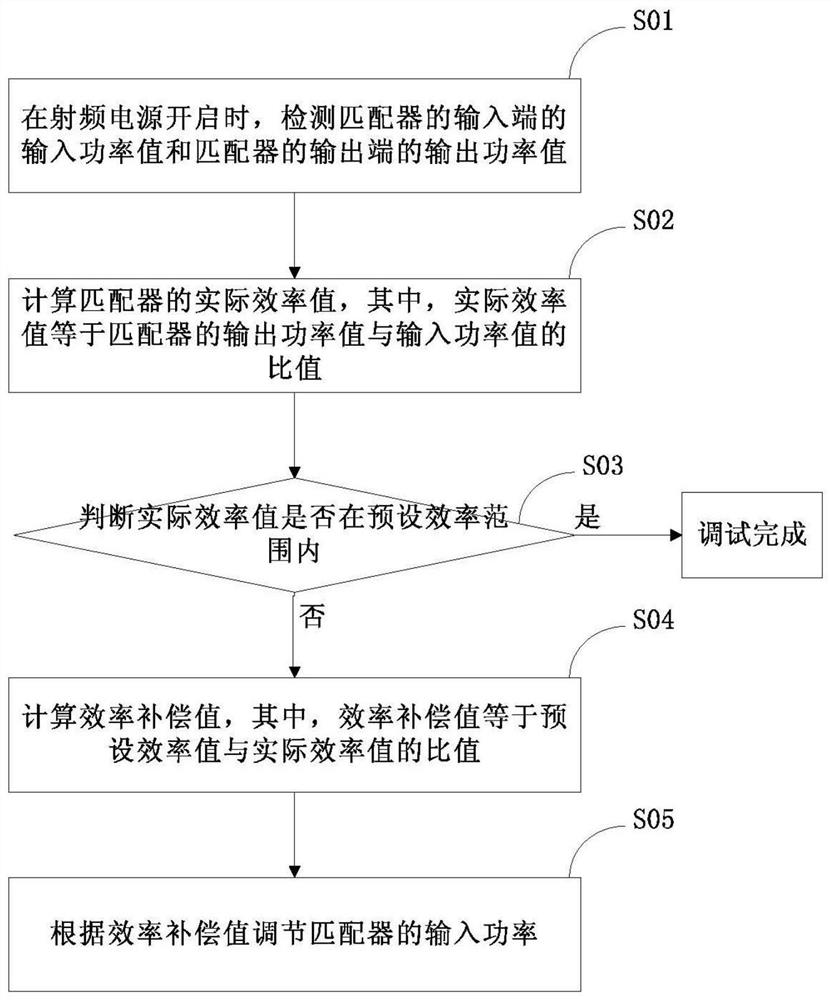
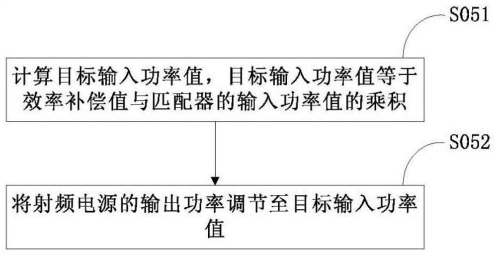
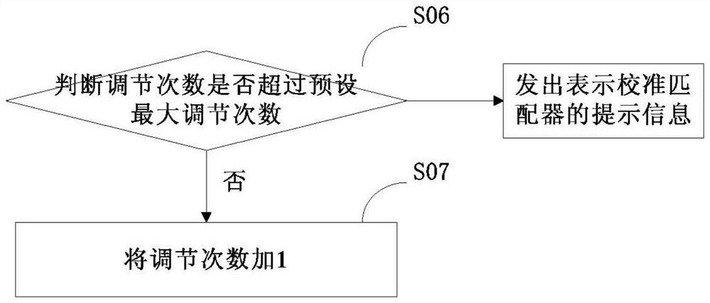
[0038] In order to realize the object of the present invention, a method for debugging the output power of a matcher is provided. Specifically, the input end of the matcher is electrically connected to the output end of the RF power supply, and the output end of the matcher is electrically connected to the RF power receiving end of the process chamber (such as the upper electrode coil or the lower electrode of the process chamber); The device is used to feed the RF power output by the RF power supply into the reaction chamber. However, since the matcher has a certain loss of its own, the actual power fed into the reaction chamber through the matcher will be far from the actual output power of the RF power supply, and the losses of different matchers are different. If different matchers are put into use, the quality consistency of the manufactured wafers cannot be guaranteed. In order to solve the above technical problems, such as figure 1 As shown, the debugging method provi...

Embodiment 2

[0075] This embodiment provides a debugging system for debugging the output power of the matcher, such as Figure 6 As shown, it includes a power detection unit 2 and a control unit 1 .

[0076] Wherein, the power detection unit 2 is used to detect the input power value of the input end of the matching device 4 and the output power value of the output end of the matching device 4 when the radio frequency power supply 3 is turned on, and send the input power value and the output power value of the matching device 4 to control unit 1. In some embodiments, when the matcher 4 is applied in the field of semiconductor processing, the input end of the matcher 4 is electrically connected to the output end of the radio frequency power supply 3. At this time, the input power value of the input end of the matcher 4 is the radio frequency The output power value of the power supply 3 ; the output end of the matcher 4 is electrically connected to the components (eg, the bottom electrode) i...


PUM


Abstract

The invention provides a matcher output power debugging method and a debugging system. The debugging method specifically comprises the following steps of when a radio frequency power supply is turned on, detecting an input power value of an input end of a matcher and an output power value of an output end of the matcher, calculating the actual efficiency value of the matcher, wherein the actual efficiency value is equal to the ratio of the output power value to the input power value of the matcher, judging whether the actual efficiency value is within a preset efficiency range or not, if not, calculating an efficiency compensation value, enabling the efficiency compensation value to be equal to the ratio of the preset efficiency value to the actual efficiency value, and adjusting the input power of the matcher according to the efficiency compensation value. According to the matcher output power debugging method and the debugging system provided by the invention, the required output power can be obtained through relatively few debugging times, so that the resource consumption for debugging can be reduced, and the debugging time can be shortened.

Description

technical field [0001] The present invention relates to the field of semiconductor manufacturing, in particular to a method and system for debugging the output power of a matcher. Background technique [0002] Currently, plasma surface treatment technology is widely used in the field of semiconductor manufacturing. The plasma surface treatment process is usually by exciting the plasma in the process chamber and applying a certain radio frequency power on the wafer to attract the specified plasma deposition or bombard the surface of the wafer, so as to complete the coating or etch. Among them, the RF power involved in the process is generated by the RF power supply and matched into the chamber through the matcher. However, due to the power loss of the matcher itself, the actual amount of RF power matched into the chamber is unknown. Moreover, there are differences in efficiency between different matchers. Therefore, in order to ensure the consistency of product quality, it ...

Claims


Application Information

Patent Timeline
Patent Type & Authority Applications(China)
IPC IPC(8): H01J37/32
CPCH01J37/32183H01J2237/332H01J2237/334
Inventor 岳昕钟晨玉卫晶
Owner BEIJING NAURA MICROELECTRONICS EQUIP CO LTD
Why Eureka
Try Eureka