Packaging structure of MEMS pressure sensor

A pressure sensor and packaging structure technology, applied in microstructure technology, microstructure devices, measuring fluid pressure, etc., can solve problems such as signal interference, achieve the effects of improving reliability, improving processing quality and efficiency, and reducing process difficulty

Active Publication Date: 2021-10-22
ANHUI BEIFANG XINDONG LIANKE MICROSYST TECH +1
View PDF15 Cites 2 Cited by
  • Summary
  • Abstract
  • Description
  • Claims
  • Application Information

AI Technical Summary

Problems solved by technology

After the PAD of the MEMS pressure sensor chip 15 is connected to the PAD on the PCB board 12 through the metal lead wire 14, it is connected to the ASIC chip 17 through the metal lead wire 16. Since the pressure sensor chip 15 is not directly connected to the ASIC chip 17, the signal will be subject to certain pressure. degree of interference

Method used


Image

  • Packaging structure of MEMS pressure sensor
  • Packaging structure of MEMS pressure sensor
  • Packaging structure of MEMS pressure sensor

Examples


Embodiment 1

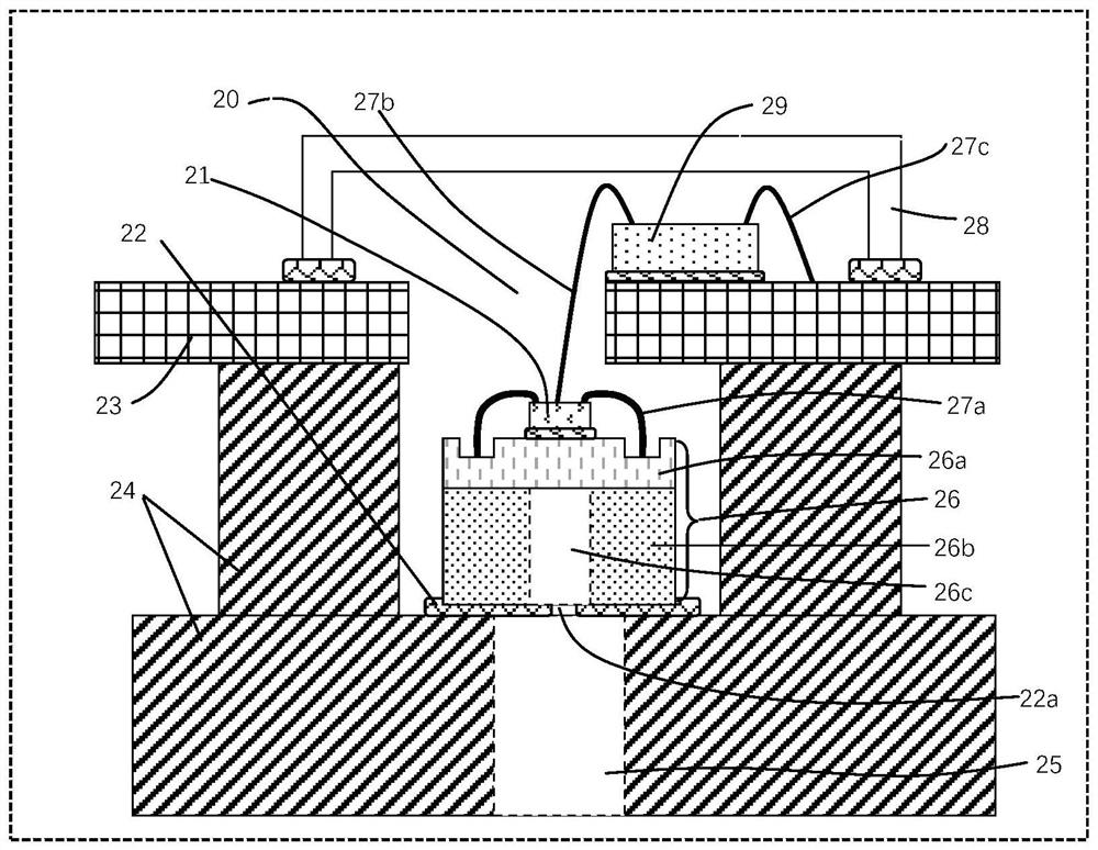
[0028] A package structure of a MEMS pressure sensor, such as figure 2 As shown, it includes a metal base 24, a MEMS pressure sensor chip 26, a PCB board 23, an adapter plate 21, an ASIC chip 29 and a cover plate 28, and the metal base 24 (commonly stainless steel, according to the needs of the application scene, such as water-resistant steam, salt spray resistance, etc., can be different grades of stainless steel, such as 304, 420, etc.) There is a cavity 20 inside, and the cavity 20 is used to install the MEMS pressure sensor chip 26. There is a vent hole 25 on the metal base 24. One end of the air hole 25 communicates with the outside world, and the other end communicates with the cavity 20 for receiving external environmental pressure (air pressure or hydraulic pressure). According to application requirements, the air hole 25 can be made into different interfaces, such as G1 / 4 internal (external) thread, etc. .

[0029] The MEMS pressure sensor chip 26 uses silicon proce...

Embodiment 2

[0035] The packaging structure of the MEMS pressure sensor of the present embodiment is as follows Figure 5 As shown, compared with the embodiment, this embodiment only removes part of the PCB board 23e extending from the metal base 24 to the adapter plate 21, and the first metal lead 27a is connected to the adapter plate from the MEMS pressure sensor chip 26 21. The second metal lead 27b is connected to the ASIC chip 29 from the adapter board 21, and the third metal lead 27c is led out from the ASIC chip 29 to the PCB board 23, and connected to the subsequent circuit.

Embodiment 3

[0037] Compared with the second embodiment, this embodiment reduces the height 24a of the metal base 24 to achieve the purpose of further reducing the wire bonding height, as Figure 6 shown.


PUM

PropertyMeasurementUnit
thicknessaaaaaaaaaa

Abstract

The invention relates to a packaging structure of an MEMS pressure sensor, which comprises a base, an MEMS pressure sensor chip, a PCB (Printed Circuit Board), an ASIC (Application Specific Integrated Circuit) chip and a cover plate, and is characterized in that an adapter plate is additionally arranged on the MEMS pressure sensor chip, and double-row or multi-row leads on the MEMS pressure sensor chip are converted into single-row leads, so that the process difficulty can be reduced when the MEMS pressure sensor chip is connected with the ASIC chip; the adapter plate is additionally arranged on the MEMS pressure sensor chip, and one-time routing is divided into two-time routing, so the vertical height of a metal lead is reduced, the process difficulty of a product is reduced, and the reliability of the product is improved; moreover, a temperature sensor can be manufactured on the adapter plate, and a temperature reference is provided for calibrating the performance of the pressure sensor device.

Description

technical field [0001] The invention belongs to the field of micro-electromechanical technology, and in particular relates to a package structure of a MEMS pressure sensor. Background technique [0002] The pressure sensor senses the pressure signal through the pressure sensitive unit, and converts the pressure signal into an available output electrical signal according to certain rules, and then is processed by the signal processing unit into the corresponding analog output or digital output form. With the rapid growth of handheld devices, the shipments of pressure sensors based on MEMS technology have increased significantly. Pressure sensors based on micro-electromechanical technology (MEMS) technology mainly include piezoresistive, capacitive and resonant. Hereinafter collectively referred to as the pressure sensor chip). Since the pressure sensor is used in a harsh environment, it needs to be compatible with complex media environments such as water, oil, compressed air...

Claims


Application Information

Patent Timeline
Patent Type & Authority Applications(China)
IPC IPC(8): B81B7/00B81B7/02G01L19/00G01L19/04
CPCB81B7/02B81B7/007B81B7/0087G01L19/00G01L19/0061G01L19/0092G01L19/04B81B2201/0264G01L2019/0053
Inventor 苏佳乐刘金锋华亚平
Owner ANHUI BEIFANG XINDONG LIANKE MICROSYST TECH
Why Eureka
Try Eureka