Method for testing corresponding relation among service life, sample thickness and body service life of N-type silicon wafer

A technology of sample thickness and corresponding relationship, which is applied in semiconductor working life testing, single semiconductor device testing, semiconductor characterization, etc., can solve the problems of inaccurate calculation of real body life, large value deviation, etc., and achieve good control of silicon polishing Effects of Feminity Lifespan

Active Publication Date: 2021-10-26
MCL ELECTRONICS MATERIALS
View PDF12 Cites 0 Cited by
  • Summary
  • Abstract
  • Description
  • Claims
  • Application Information

AI Technical Summary

Problems solved by technology

[0004] However, when testing silicon wafer samples of different thicknesses, the value of the test life often deviates greatly from the value of the real life of the silicon wafer samples. The test life measured by means cannot accurately calculate its real body life;

Method used


Image

  • Method for testing corresponding relation among service life, sample thickness and body service life of N-type silicon wafer
  • Method for testing corresponding relation among service life, sample thickness and body service life of N-type silicon wafer
  • Method for testing corresponding relation among service life, sample thickness and body service life of N-type silicon wafer

Examples


Embodiment Construction

[0034] Regarding the aforementioned and other technical contents, features and effects of the present invention, refer to the appended Figures 1 to 6 Examples will be described in detail.

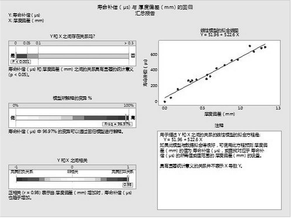
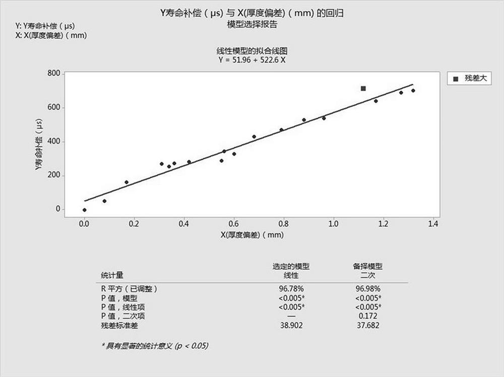
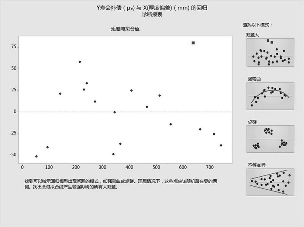
[0035] In the existing test methods for the minority carrier lifetime of silicon wafers, the microwave photoconductive decay method is usually used, that is, it mainly includes the two processes of laser injection to generate electron-hole pairs and microwave detection signal changes. The 904nm laser injection (for Silicon, the implantation depth is about 30um) to generate electron-hole pairs, resulting in an increase in the conductivity of the sample. When the external light injection is removed, the conductivity decays exponentially with time. This trend indirectly reflects the decay trend of minority carriers, thus The lifetime of minority carriers can be obtained by detecting the trend of conductivity with time through microwave;

[0036] However, the above test process is affected by...


PUM

PropertyMeasurementUnit
thicknessaaaaaaaaaa
electrical resistivityaaaaaaaaaa

Abstract

The invention relates to a method for testing the corresponding relation among the service life, the sample thickness and the body service life of an N-type silicon wafer. The method effectively solves the problem that the measured service life is greatly deviated from the real body service life when the service life of a silicon wafer with small thickness is measured in the prior art. According to the technical scheme, the corresponding relation among the test service life, the sample thickness and the body service life is obtained by testing the corresponding relation among the test service life, the sample thickness and the body service life of the N-type silicon wafer, and the body service life of the sample can be accurately calculated by measuring the test service life of the silicon wafer of any thickness according to the scheme. Therefore, the effect of better controlling the minority carrier lifetime of the silicon polished wafer is realized.

Description

technical field [0001] The invention belongs to the technical field of silicon wafer detection, and in particular relates to a method for the corresponding relationship between N-type silicon wafer test life, sample thickness and body life. Background technique [0002] Minority carrier lifetime is an important parameter of semiconductor materials and devices. It directly reflects the quality of the material and the characteristics of the device. Accurately obtaining this parameter is of great significance for the manufacture of semiconductor devices; [0003] The microwave photoconductivity decay method is a standard method for measuring semiconductor materials. The microwave photoconductivity decay method (Microwave photoconductivity decay) tests the minority carrier lifetime, mainly including the two processes of electron-hole pairs generated by laser injection and changes in microwave detection signals. 904nm laser implantation (for silicon, the implantation depth is ab...

Claims


Application Information

Patent Timeline
Patent Type & Authority Applications(China)
IPC IPC(8): G01R31/26G06F17/18
CPCG01R31/2642G01R31/2648G06F17/18Y02P70/50
Inventor 方丽霞张奇田素霞张倩刘丽娟
Owner MCL ELECTRONICS MATERIALS
Why Eureka
Try Eureka