Flatness control method and device, and coating film forming method and device

A control method and a technology of a control device, which are applied in the direction of bonding methods, film/sheet adhesives, photoplate-making process coating equipment, etc., can solve problems such as uneven processing, and achieve the effect of reducing the variation of coating film thickness Effect

Pending Publication Date: 2021-10-26
SHIN ETSU CHEM IND CO LTD
View PDF7 Cites 0 Cited by
  • Summary
  • Abstract
  • Description
  • Claims
  • Application Information

AI Technical Summary

Problems solved by technology

[0008] In addition, it is not limited to the case of forming a coating film. When the wafer is held and processed, since the wafer is not held flat, processing will be applied unevenly within the wafer surface. Holding the wafer flat becomes a problem

Method used


Image

  • Flatness control method and device, and coating film forming method and device
  • Flatness control method and device, and coating film forming method and device
  • Flatness control method and device, and coating film forming method and device

Examples


Embodiment 1

[0200] In Example 1, the flatness of the wafer was controlled by the following procedure.

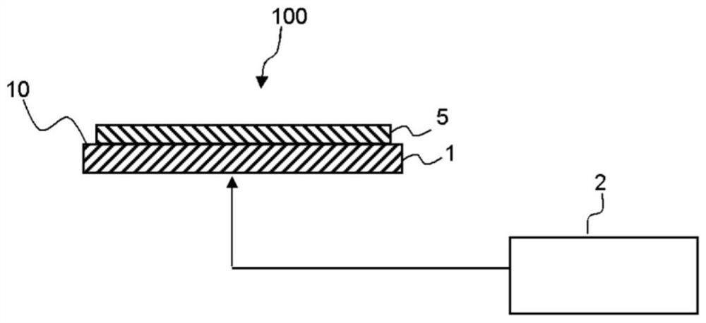
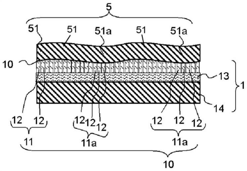
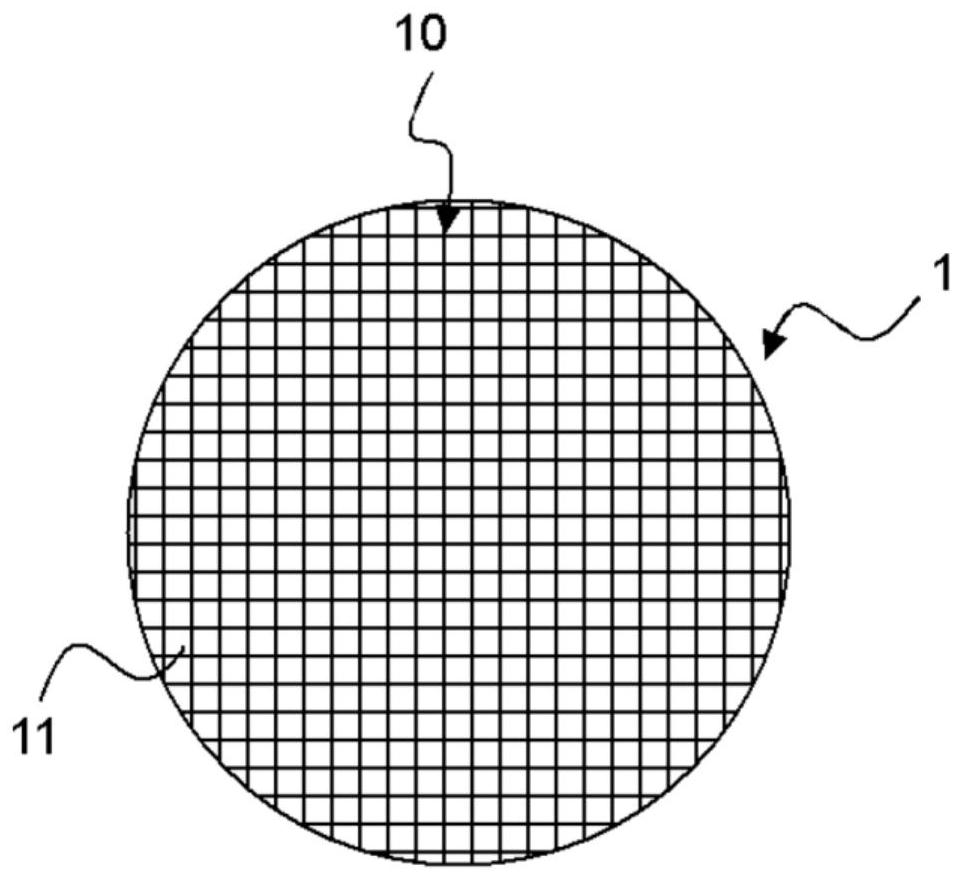
[0201] First, prepare and Figure 1 ~ Figure 3 The same flatness control device 100 is shown. The holding surface 10 includes configurations such as image 3 A thousand segments 11 of a checkerboard grid are shown. Also, the dry adhesive fibrous structure 12 of the holding member 1 has Figure 5 The shape shown roughly.

[0202] Next, the wafer 5 to be controlled is prepared. Wafer 5 contains a thousand silicon wafers of divided regions 51 .

[0203] Such as figure 2 As shown, the wafer 5 is adsorbed on the holding surface 10 of the holding member 1 , and the wafer 5 is held on the holding member 1 .

[0204] In this state, the flatness of each of the divided regions 51 of the wafer 5 is measured, and information on the flatness is acquired. The flatness of wafer 5 was 0.4 microns.

[0205] Next, the controller 2 judges, among the plurality of divided regions 51 of the wafer 5...

Embodiment 2

[0208] In Example 2, the flatness of the wafer was controlled in the same procedure as in Example 1 except for the following points.

[0209] In the second embodiment, the flatness information of the wafer 5 is obtained by measuring the flatness before being held by the holding member 1 , and based on this information, the flatness is controlled in the same manner as in the first embodiment. The flatness of the wafer 5 held in front of the holding member 1 is 0.01 μm. Also, in Example 2, the same wafer 5 as that in Example 1 was used.

[0210] The flatness of the wafer 5 whose flatness is controlled in Example 2 is 0.01 μm.

Embodiment 3

[0212] In Example 3, on the wafer 5 whose flatness was controlled in Example 1, a photoresist film was formed by the following procedure.

[0213] Such as Figure 7 As shown, the wafer 5 whose flatness has been controlled is held by the holding member 1 , and is fixed by the vacuum chuck 4 .

[0214] Next, the test coating film-forming composition was coated on the wafer 5 in this state using the coating device 6 . A photoresist was used as the composition for test coating film formation.

[0215] Next, it baked at 100 degreeC, and formed the photoresist film.


PUM

PropertyMeasurementUnit
surface smoothnessaaaaaaaaaa

Abstract

The invention provides a flatness control method and apparatus, and a coating film forming method and apparatus. The flatness control method provided by the invention is used for controlling the flatness of the wafer. The method includes: a step of preparing a holding member having a holding surface including a plurality of segments, each of the plurality of segments being provided with a dry adhesive fiber structure; a step of absorbing a wafer on the holding surface of the holding member and holding the wafer on the holding member; measuring the flatness of the wafer to obtain information on the flatness of the wafer; and releasing the suction of the wafer by the dry adhesive fiber structure in a part of the plurality of sections of the holding surface of the holding member on the basis of the flatness information.

Description

technical field [0001] The present invention relates to a flatness control method, a coating film forming method, a flatness control device, and a coating film forming device. Background technique [0002] With the high integration and high speed of large-scale integrated circuits (LSI), how to use photolithography using chemically amplified photoresist, which is currently used as a general-purpose technology, in today's world where miniaturization of pattern specifications is required Various technologies have been developed for finer and high-precision pattern processing of light sources. [0003] In photolithography using a chemically amplified photoresist, a wafer, which is a to-be-processed object, is fixed, and a chemically amplified photoresist film-forming material is applied in the fixed state. It is known that wafers are fixed by widely used methods such as vacuum adsorption and electrostatic adsorption, or methods using adhesive films or sheets (for example, Pate...

Claims


Application Information

Patent Timeline
Patent Type & Authority Applications(China)
IPC IPC(8): G03F7/16
CPCG03F7/162G03F7/16G03F7/707G03F7/70733G03F7/7095H01L21/6875C09J7/00C09J2301/31C09J5/00C09J2301/502C09J2203/326H01L21/683H01L21/67288H01L22/12H01L21/6715G03F7/70783G03F7/7085H01L21/67253H01L21/6836H01L2221/68322H01L2221/68381
Inventor 荻原勤
Owner SHIN ETSU CHEM IND CO LTD
Why Eureka
Try Eureka