Eureka AIR delivers breakthrough ideas for toughest innovation challenges, trusted by R&D personnel around the world.

Miniaturized heavy-load solid-state relay

A solid-state relay, large-load technology, applied in the direction of logic circuits using optoelectronic equipment, logic circuits using specific components, etc., can solve the problems of weak photovoltaic driving capability, limited parallel connection, and small photovoltaic driving current, etc., to meet the requirements of equipment miniaturization. , the overall volume miniaturization, the effect of reducing product volume

Pending Publication Date: 2021-10-26
GUIZHOU SPACE APPLIANCE CO LTD
View PDF12 Cites 0 Cited by
  • Summary
  • Abstract
  • Description
  • Claims
  • Application Information

AI Technical Summary

Problems solved by technology

Nowadays, conventional optical MOS relays use photovoltaics to drive MOS chips. For example, a solid relay provided by a Chinese patent with a publication number of CN103516343A is difficult to drive a large-load MOS chip due to the weak driving ability of photovoltaics. Because the MOS chip with a large load has a large junction capacitance, and the photovoltaic drive current is small
If you want to improve its driving ability, you generally need to improve its driving ability through a driving circuit, such as an optical coupling device provided by a Chinese patent with a publication number of CN101872761A, which achieves improving driving ability by connecting multiple light-receiving elements (photovoltaics) in parallel However, this kind of parallel connection is very limited, because the driving current of the light-receiving element is generally several microamperes to tens of microamperes. If it is necessary to drive a large load, it cannot meet the requirements, and after multiple parallel connections, its volume is bound to increase. Can not meet the needs of miniaturization and large load

Method used


Image

  • Miniaturized heavy-load solid-state relay
  • Miniaturized heavy-load solid-state relay
  • Miniaturized heavy-load solid-state relay

Examples


Embodiment

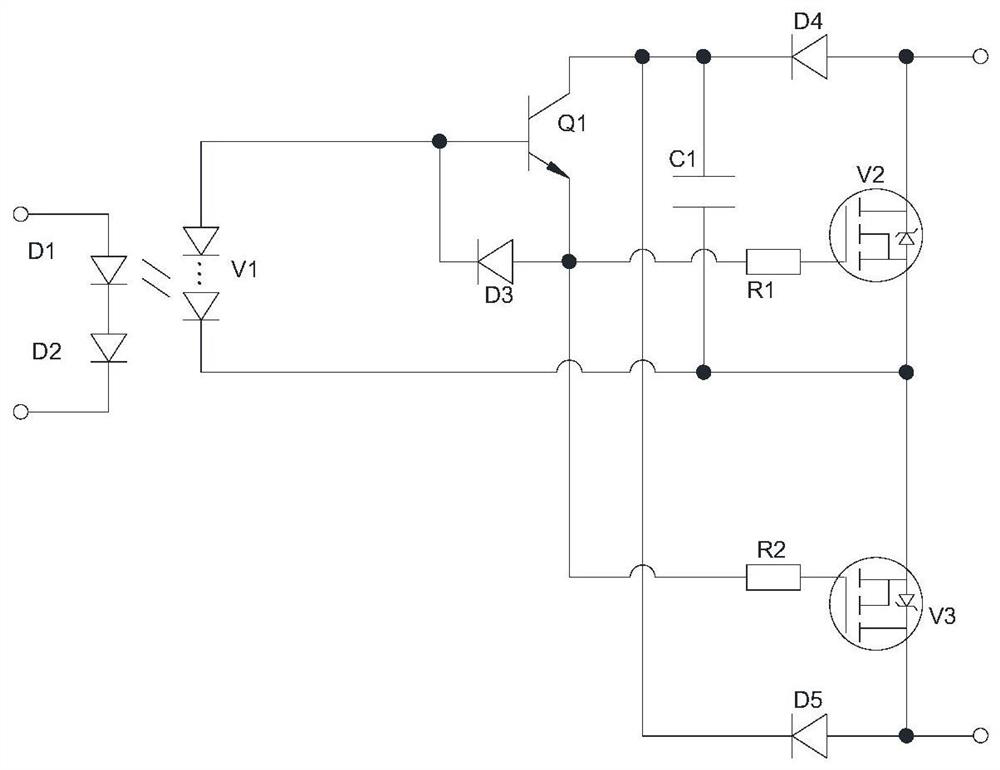
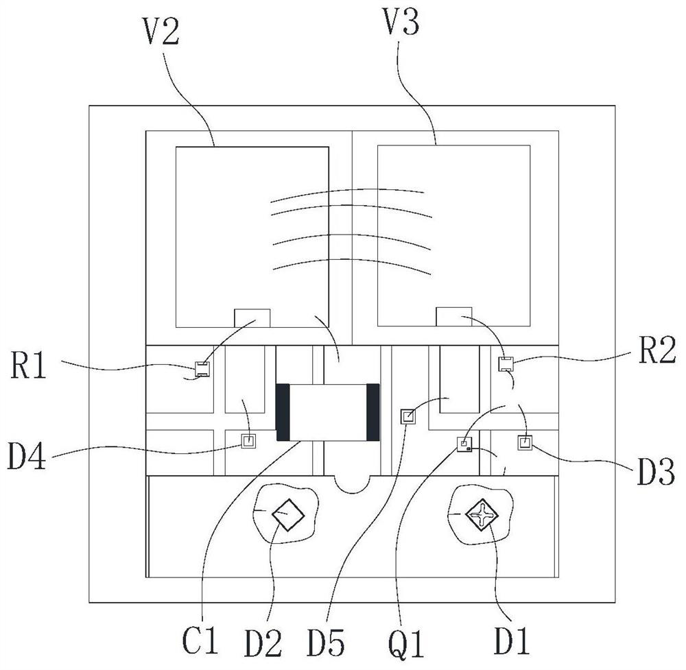
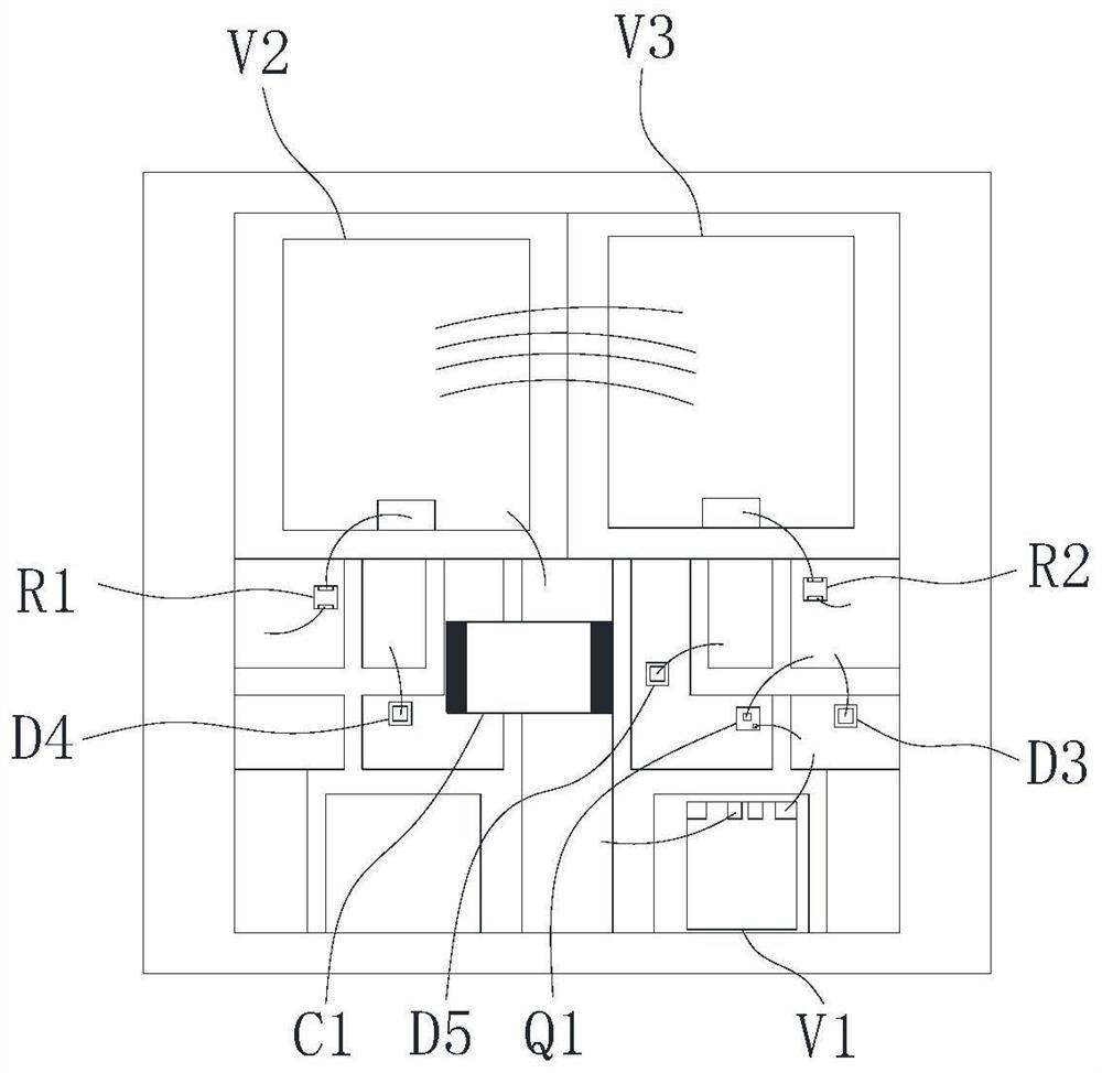
[0037] A solid-state relay with miniaturization and large load. In order to achieve fast on-off and improve driving capability, its driving circuit is as follows: figure 1 As shown, it consists of light-emitting diode D1, switching diodes D2, D3, D4 and D5, photovoltaic V1, transistor Q1, capacitor C1, resistors R1, R2, and MOS chips V2 and V3. Light-emitting diode D1 is connected to the input power supply for photovoltaic V1. The light drive signal, the output anode of the photovoltaic V1 is connected to the source of the MOS chip V2, the drain of the MOS chip V2 is connected to the anode of the switching diode D4, and a capacitor C1 is connected in parallel between the cathode of the switching diode D4 and the source of the MOS chip V2. The cathode of the switching diode D4 is connected to the collector of the transistor Q1, the base of the transistor Q1 is connected to the output cathode of the photovoltaic V1, a resistor R1 is connected in series between the gate of the MOS c...


PUM


Abstract

The invention provides a miniaturized heavy-load solid-state relay, which comprises a tube shell, an inner ceramic chip and a driving circuit, and is characterized in that the driving circuit is provided with a light-emitting diode D1 and a photovoltaic V1 to form a driving control circuit, and the driving control circuit is isolated through light; a triode Q1, a capacitor C1 and a switching diodes D4 and D5 form an amplification charging circuit; the switching diode D3 and the photovoltaic V1 form a bleeder circuit; MOS chips V2 and V3 form a switching circuit; components are each of a surface-mounted structure and are interconnected by using a bonding process; the tube shell and the inner ceramic chip are each provided with a plurality of electrode bonding pads; the light-emitting diode D1 and the switching diode D2 are respectively and fixedly attached to the electrode bonding pads of the inner ceramic chip; the other components are respectively and fixedly attached to the electrode bonding pads of the tube shell; the inner ceramic chip is buckled on the tube shell; and the light-emitting diode D1 is aligned with the photovoltaic V1. According to the miniaturized heavy-load solid-state relay provided by the invention, by designing the rapid charging and discharging circuit, the product size is reduced, and meanwhile, the driving capability of the relay is improved.

Description

technical field [0001] The invention belongs to the technical field of relays, and in particular relates to a solid-state relay with miniaturization and large load. Background technique [0002] For a relay, a relay is a switch with input and output isolation. Generally speaking, small size and load capacity are the goals that relays are constantly pursuing. Now, the smallest type of relay is the optical MOS relay packaged in ceramics. To increase its load capacity, its driving capacity must be improved. Only when the driving capacity is improved can it provide protection for large loads. Nowadays, conventional optical MOS relays use photovoltaics to drive MOS chips. For example, a solid relay provided by a Chinese patent with a publication number of CN103516343A is difficult to drive a large-load MOS chip due to the weak driving ability of photovoltaics. Because the MOS chip with a large load has a large junction capacitance, and the photovoltaic drive current is small. ...

Claims


Application Information

Patent Timeline
Patent Type & Authority Applications(China)
IPC IPC(8): H03K19/14
CPCH03K19/14
Inventor 田知静舒德兵余贵龙裴雨滋
Owner GUIZHOU SPACE APPLIANCE CO LTD
Why Eureka
Eureka Blog
Learn More