A non-destructive storage device for silicon wafers used in the manufacture of communication electronic products

A technology for electronic products and storage devices, applied in the field of communication electronic materials, can solve the problems of rolling out damage of silicon wafers inside the device, affecting the use effect of silicon wafers, poor protection effect of silicon wafers, etc. The effect of colliding with each other and reducing economic losses

Active Publication Date: 2021-12-14
徐州和润电子材料有限公司
View PDF19 Cites 0 Cited by
  • Summary
  • Abstract
  • Description
  • Claims
  • Application Information

AI Technical Summary

Problems solved by technology

[0005] In order to solve the above-mentioned technical problems, the present invention provides a non-destructive storage device for silicon wafers used in the manufacture of communication electronic products to solve the problem that the existing similar silicon wafer storage devices used in the manufacture of communication electronic products have poor protection effect on silicon wafers. When the outside is hit by an external force, it is very easy to cause the internal silicon chip to be broken due to excessive force, and the storage device is easily stored upside down due to human negligence, causing the silicon chip inside the device to roll out and be damaged, affecting the use effect of the silicon chip

Method used


Image

  • A non-destructive storage device for silicon wafers used in the manufacture of communication electronic products
  • A non-destructive storage device for silicon wafers used in the manufacture of communication electronic products
  • A non-destructive storage device for silicon wafers used in the manufacture of communication electronic products

Examples


Embodiment 1

[0044] as attached figure 1 to attach Figure 10 Shown:

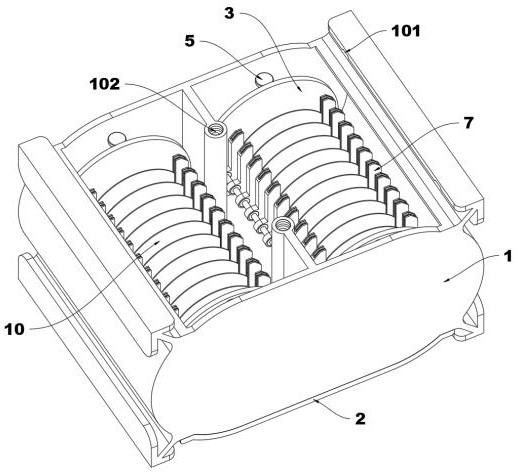
[0045]The invention provides a non-destructive storage device for silicon wafers used in the manufacture of communication electronic products, which includes a housing 1, a receiving plate 3, a connector 5 and a U-shaped storage rack 7; the inside of the housing 1 is a hollow structure, and a sealing cover 2 is buckled on the housing 1 Access ports at the upper and lower ends; the receiving plate 3 is installed symmetrically at the front and rear ends of the shell 1, and the inner sides of the two receiving plates 3 are connected to each other through the support rod 4; the connecting piece 5 is installed symmetrically inside the shell 1 The front and rear ends, and the connecting piece 5 is connected with the receiving plate 3; the U-shaped storage rack 7 is arranged and installed inside the shell 1, and the U-shaped storage rack 7 is connected with the support rod 4 through the magnetic ring 9; the two ends of the su...

Embodiment 2

[0048] Wherein, the connectors 5 are rotatably connected to the inner sides of the front and rear ends of the housing 1, and the outer ring 301 is attached to the inner side of the housing 1; with the above-mentioned technical scheme, when the housing 1 is stored and transported upside down, the U-shaped storage rack 7 is automatically rotated under the influence of gravity, Make the top of the U-shaped storage rack 7 face upwards all the time, prevent the silicon wafer 10 inside the U-shaped storage rack 7 from rolling out, and ensure the storage stability of the silicon wafer 10 inside the U-shaped storage rack 7 .

Embodiment 3

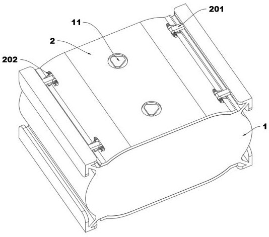
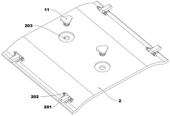
[0050] Among them, the upper and lower ends of the housing 1 are left and right symmetrically provided with four limit slots 101, and the top of the sealing cover 2 is symmetrically rotated and connected with four clamping blocks 201, and the top of the clamping block 201 is clamped on the limit position. In the groove 101, the torsion spring 202 is set on the outside of both ends of the clamping block 201, the bottom of the torsion spring 202 is attached to the top side of the sealing cover 2, one end of the torsion spring 202 is attached to the bottom side of the clamping block 201, and the upper and lower ends of the housing 1 are respectively A screw hole 102 is opened, and a connecting hole 203 is opened symmetrically inside the sealing cover 2. The connecting hole 203 communicates with the screw hole 102. The special-shaped bolt 11 is connected in the connecting hole 203, and the bottom end of the special-shaped bolt 11 is threadedly connected to the screw hole 102. Insid...


PUM


Abstract

The invention provides a non-destructive storage device for silicon wafers used in the manufacture of communication electronic products, which relates to the field of communication electronic materials and includes a U-shaped storage rack; the inside of the housing is hollow, and the sealing cover is buckled at the access opening on the top of the housing; The receiving plate is symmetrically installed at the front and rear ends of the shell, and the inner sides of the two receiving plates are connected to each other through support rods; the connecting piece is symmetrically installed at the front and rear ends of the shell, and the connecting piece is connected with the receiving plate ; The U-shaped storage racks are arranged and installed inside the shell; a U-shaped cotton tank is installed inside the U-shaped storage rack, and the silicon wafer is slidably inserted in the U-shaped cotton tank; when the front and rear sides of the shell are subjected to external forces When impacted, the U-shaped storage rack slides back and forth inside the shell to offset the impact force. Using the same-sex repulsion principle of magnets, the U-shaped storage rack slides and resets itself through magnetic force, ensuring the storage effect of silicon chips inside the U-shaped storage rack.

Description

technical field [0001] The invention belongs to the technical field of communication electronic materials, and more specifically relates to a non-destructive storage device for silicon wafers used in the manufacture of communication electronic products. Background technique [0002] Silicon wafers, also known as wafers, are processed from silicon ingots. Millions of transistors can be etched on silicon wafers through special processes. They are widely used in the manufacture of communication and electronic products. Because silicon wafers are easy to Because of its crushing characteristics, special storage devices are usually required for storage and transportation. [0003] The storage device for silicon wafers used in the manufacture of communication electronic products can refer to patent CN210025214U, which mainly includes a top plate and a bottom plate; a sliding plate, the top and bottom of the sliding plate slide between the opposite sides of the top plate and the bot...

Claims


Application Information

Patent Timeline
Patent Type & Authority Patents(China)
IPC IPC(8): B65D25/02B65D81/05B65D85/62B65D85/90B65D81/07B65D55/02B65D81/18B65D85/30
CPCB65D25/02B65D81/05B65D85/62B65D81/07B65D55/02B65D81/18B65D85/30B65D2585/86
Inventor 徐建萍
Owner 徐州和润电子材料有限公司
Why Eureka
Try Eureka