
Eureka
For R&D, Eureka makes reading and utilizing patents & technical documents easy.
Eureka AIR
Designed for self-driven R&D workflows. Generate viable solutions, solve complex R&D challenges, empower your innovation with AI.

Eureka Materials
Designed for material experts only. Revolutionize your material R&D, from search, analyze, to developing new materials.

TechResearch
Generate reliable direction feasibility study reports for your R&D in just a few steps.

TechSeek
Discover and master advanced knowledge NOW. Basics, ideas, possibilities, all at once.

TechMind
As an expert in R&D Theories, TechMind can generates customized viable solutions instantly.

TechRisk
Analyze your overall solution with one click, know your potential R&D risks in advance.

TechMonitor
Get weekly tech updates, stay abreast of the latest tech innovations and key insights.
Method for forming chip packaging structure
A chip packaging structure and bare chip technology, which is applied in the manufacture of electrical components, electrical solid devices, semiconductor/solid devices, etc., can solve the problems of low yield rate of packaged products, improve product yield, prevent dielectric layer breakage, Avoid the effect of height gap
- Summary
- Abstract
- Description
- Claims
- Application Information
AI Technical Summary
Problems solved by technology
Method used
Image

Examples
Embodiment Construction
[0073] In order to make the above objects, features and advantages of the present invention more comprehensible, specific embodiments of the present invention will be described in detail below in conjunction with the accompanying drawings.
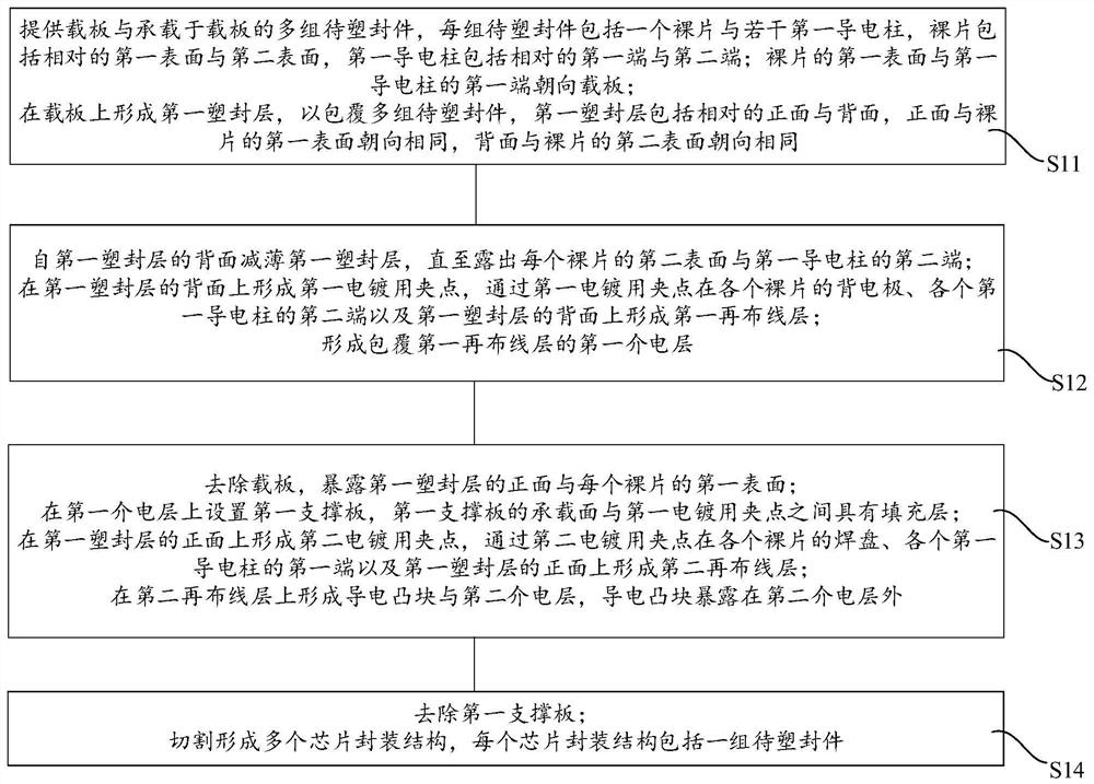
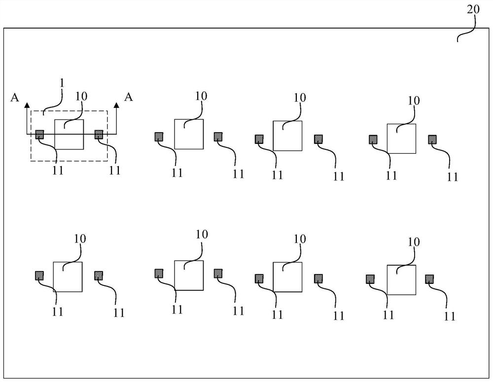
[0074] figure 1 is a flow chart of the method for forming the chip package structure according to the first embodiment of the present invention; Figure 2 to Figure 7 , Figure 9 yes figure 1 The schematic diagram of the intermediate structure corresponding to the process in . Figure 8 is a schematic diagram of the control structure.
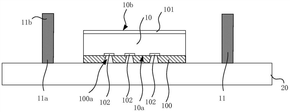
[0075] First, refer to figure 1 Step S11 in, figure 2 and image 3 As shown, a carrier board 20 and multiple groups of parts to be molded 1 carried on the carrier board 20 are provided, each group of parts to be molded 1 includes a die 10 and a plurality of first conductive pillars 11, and the die 10 includes an opposite first surface 10a With the second surface 10b, the first conductive pillar 11 i...
PUM
 Abstract
Description
Claims
Application Information
 - R&D Engineer
- R&D Manager
- IP Professional
- Industry Leading Data Capabilities
- Powerful AI technology
- Patent DNA Extraction
Browse by: Latest US Patents, China's latest patents, Technical Efficacy Thesaurus, Application Domain, Technology Topic, Popular Technical Reports.
© 2024 PatSnap. All rights reserved.Legal|Privacy policy|Modern Slavery Act Transparency Statement|Sitemap|About US| Contact US: help@patsnap.com