Check patentability & draft patents in minutes with Patsnap Eureka AI!

Adhesive circuit patterning process

A circuit pattern, pattern technology, applied in the direction of printed circuit, printed circuit, printed circuit manufacturing, etc., can solve the problems of limited repeatability and consistency, cleanable cycle, surface mount device package, low interconnect reliability, etc.

Pending Publication Date: 2021-10-29
JABLIN INC
View PDF0 Cites 0 Cited by
  • Summary
  • Abstract
  • Description
  • Claims
  • Application Information

AI Technical Summary

Problems solved by technology

Direct conductive ink screen printing has print repeatability and consistency of printed circuit patterns, is not suitable for high-density circuits and miniaturized products, has limited washable cycles that require additional waterproofing processes, and has low interaction on surface mount device packages. even reliability

Method used


Image

  • Adhesive circuit patterning process
  • Adhesive circuit patterning process
  • Adhesive circuit patterning process

Examples


Embodiment Construction

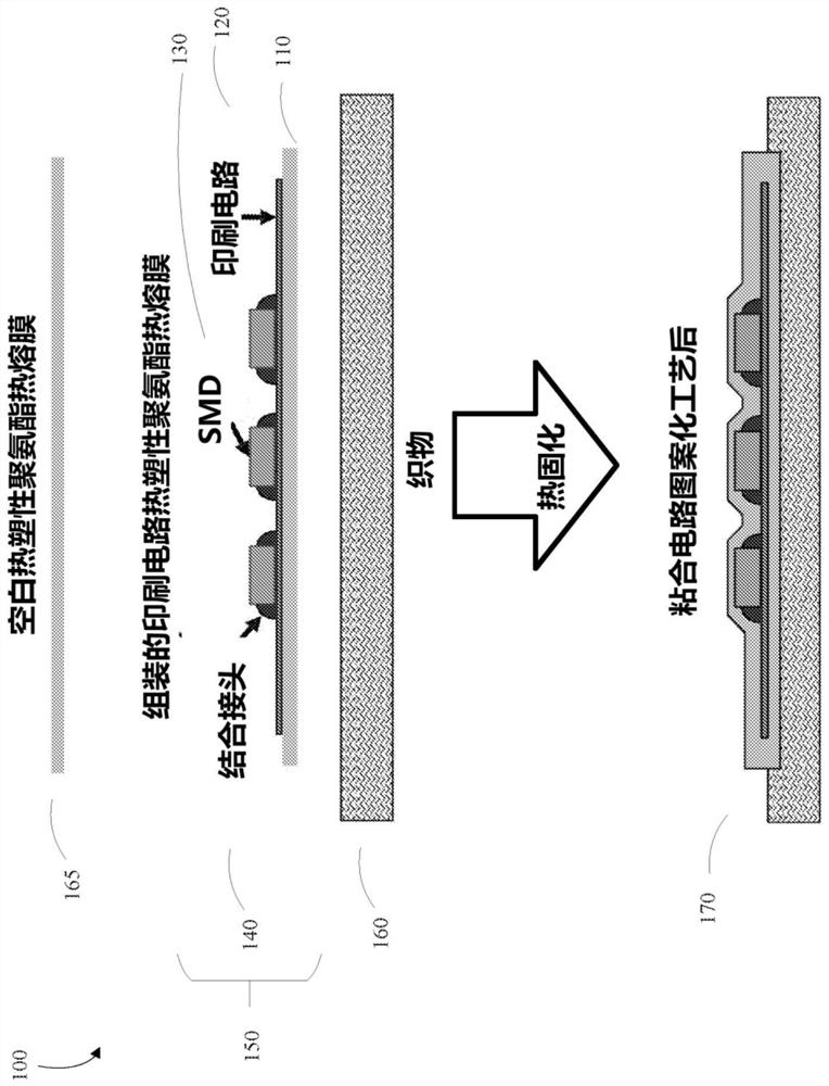
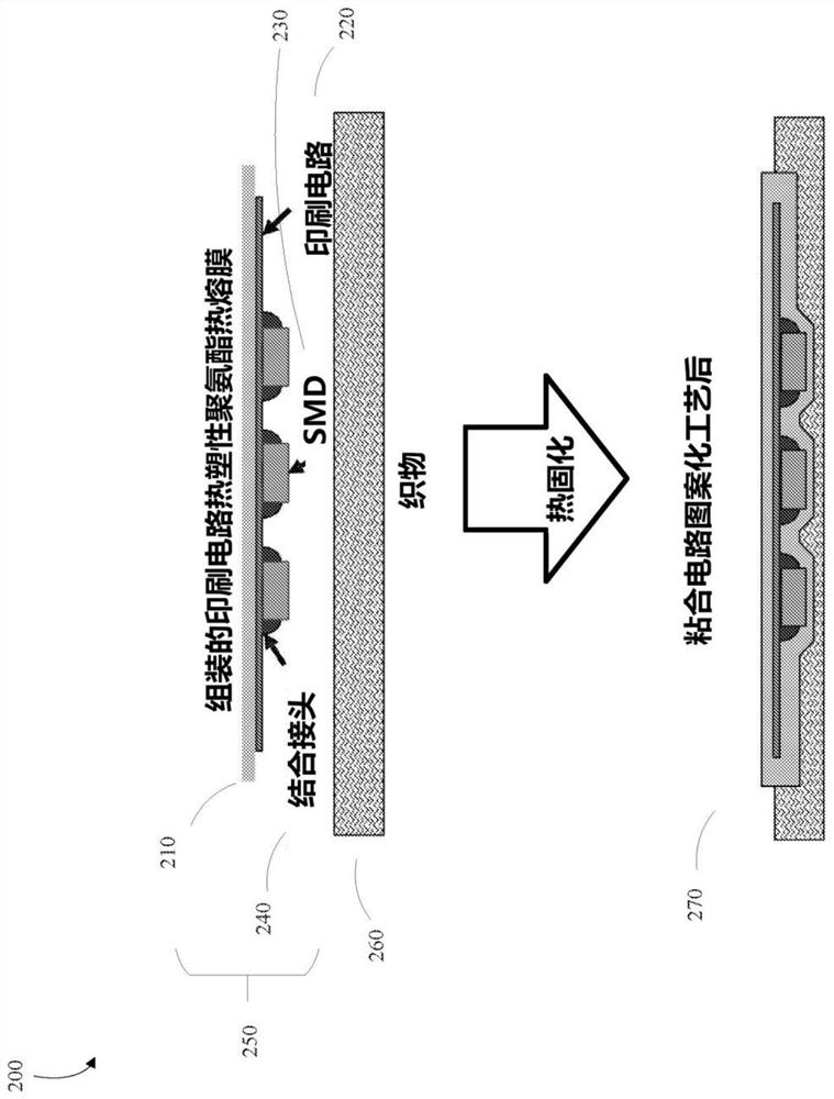
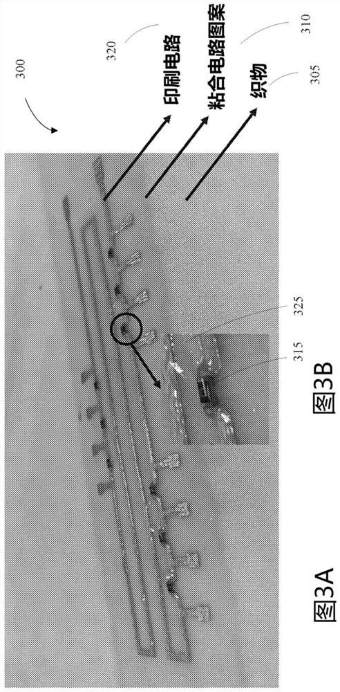
[0021] The drawings and descriptions provided herein may be simplified to illustrate those aspects of the described embodiments that are relevant to a clear understanding of the process, machine, product, and / or composition of matter disclosed herein, while eliminating, for the sake of clarity, typical Other aspects found in similar devices, systems, compositions and methods of the invention. Accordingly, those skilled in the art will recognize that other elements and / or steps may be desirable or necessary to implement the devices, systems, compositions and methods described herein. However, because these elements and steps are well known in the art, and because they do not contribute to a better understanding of the disclosed embodiments, a discussion of these elements and steps may not be provided here. However, the invention is considered to inherently include all such elements, changes and modifications to the described aspects that would come to be known to one of ordinar...


PUM


Abstract

Disclosed are processes and materials for adhesive circuit patterning which strengthen and protect the printed circuit traces and adhesive bonded joints of surface mounted devices in flexible or stretchable electronics in a single process. A method for adhesive circuit pattering include deposing a circuit pattern on a thermal adhesive film. One or more surface mounted device(s) are attached to a cured printed circuit to form an assembled printed circuit. The assembled printed circuit may be placed on a stretchable substrate. The thermal adhesive film is melted on the assembled printed circuit and the stretchable substrate to protect and reinforce the joint bonds and the circuit pattern of the assembled circuit pattern and attach the assembled printed circuit to the stretchable fabric in one melting or curing step.

Description

technical field [0001] The present invention relates to flexible electronic devices and circuits. Background technique [0002] Flexible electronics, such as printed, stretchable electronics, e-textiles, etc., undergo or suffer from bending, twisting, stretching, rolling, pushing, etc. Printed circuit traces, sensors, adhesive bond joints of surface mounted devices, etc. forming these flexible electronic devices may weaken due to mechanical strain and lead to open circuits. Traditional encapsulation processes typically used to protect the adhesive bond joints of surface mount devices employ lamination of polyethylene terephthalate (PET), polyimide (PI) and polycarbonate (PC) films Processes are often used to protect circuit traces. Therefore, a variety of different techniques are required to mitigate device failures induced by mechanical strain. [0003] Other techniques such as circuit embroidery, flocking and direct conductive ink screen printing have also been used. H...

Claims


Application Information

Patent Timeline
IPC IPC(8): H05K3/20H05K3/14H05K1/02
CPCH05K3/0058H05K1/189H05K2201/0129H05K3/284H05K1/038H05K2203/1311H05K2201/10151H05K3/305H05K1/0277H05K3/321
Inventor L·林Z·B·沙姆斯丁
Owner JABLIN INC
Features
  • R&D
  • Intellectual Property
  • Life Sciences
  • Materials
  • Tech Scout
  • Unparalleled Data Quality
  • Higher Quality Content
  • 60% Fewer Hallucinations
Learn More