Substrates for stretchable electronics and method of manufacture

a technology of electronics and substrates, applied in the direction of printed circuit manufacturing, circuit bendability/stretchability, printed circuit aspects, etc., can solve the problems of limited stretchability of such a device and interfacial problems

Active Publication Date: 2017-12-28
ARES MATERIALS INC
View PDF1 Cites 9 Cited by
  • Summary
  • Abstract
  • Description
  • Claims
  • Application Information

AI Technical Summary

Benefits of technology

[0005]In the presently disclosed subject matter, a method is provided for the fabrication of a bulk substrate with soft regions and stiff regions patterned directly into a material. Soft regions and stiff regions patterned directly into the material may reduce the presence of multi-material interfacing (e.g., adhesives, surface lamination, etc.) to achieve a similar multi-modulus substrate that may enable stretchable electronic stack fabrication. The method involves the use of a bulk material that can exhibit multi-modulus behavior that is spatially-controlled either during the synthesis of the bulk material, or as a function of the post-polymerization modification of the bulk material.

Problems solved by technology

While geometric solutions can address the flexibility of such structures (e.g., thin-film variations of such structures can accommodate smaller bending radii), the stretchability of such a device is still limited.
However, this lamination leads to interfacial issues that can manifest at intermediate and high strains of the elastomeric substrate onto which the stiff substrate materials are laminated.

Method used


Image

  • Substrates for stretchable electronics and method of manufacture
  • Substrates for stretchable electronics and method of manufacture
  • Substrates for stretchable electronics and method of manufacture

Examples


example 1

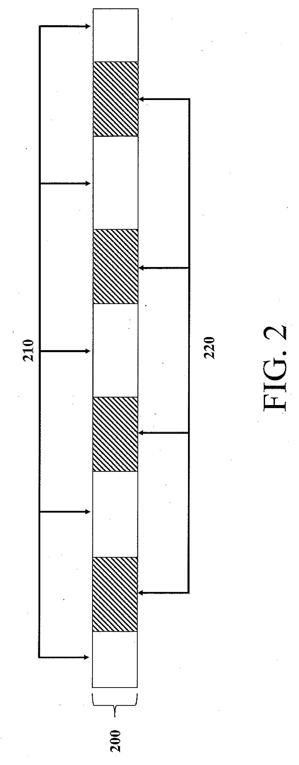
[0037]To a fluid reservoir was added the difunctional acrylate-terminated nematic liquid crystal RM 82 (Synthon) and an almost stoichiometric ratio of n-butylamine. To this solution, 1.5 wt % of the initiator 2,2-Dimethoxy-2-phenylacetophenone was added and the container was sealed, placed into the rotary mixer and mixed at 2350 rpm for 5 minutes. The monomer solution mixture was mounted to a slot-die coating tool and processed into a thin-film atop a carrier substrate with a prepatterned photoaligned dye layer via the slot-die coating technique. A secondary prepatterened photoaligned dye layer was used to cover the deposited material and allow directorate orientation across the thickness of the material. After 120 minutes, the secondary layer was removed and the material atop the carrier substrate was introduced to an ultraviolet (UV) curing oven and exposed to 10 mJ / cm̂2 of 365 nm light to initiate the polymerization, giving the final polymer film. No further spatial patterning is...

example 2

[0038]To a fluid reservoir was added the multifunctional thiol monomer Tris[2-(3-mercaptopropionyloxy)ethyl] isocyanurate (1 mol eq.) and the multifunctional co-monomer Tris(4-hydroxyphenyl)methane triglycidyl ether (1 mol eq.), and the container was sealed. The sealed container was placed into a rotary mixer and mixed at 2350 rotations per minute (rpm) for 5 minutes. The container was removed from the mixer, opened, and 1.5 wt % of the catalyst tripropylamine was pipetted dropwise into the mixed monomer solution at room temperature (about 25° C.). The container was again sealed, placed into the rotary mixer and mixed at 2350 rpm for an additional 5 minutes. Finally, the container was again removed from the mixer, opened, and the organic solvent tetrahydrofuran was added until the final solution was a 92.5% (v / v) solid-fraction monomer solution. The monomer solution mixture was mounted to a slot-die coating tool and processed into a thin-film atop a carrier substrate via the slot-di...

example 3

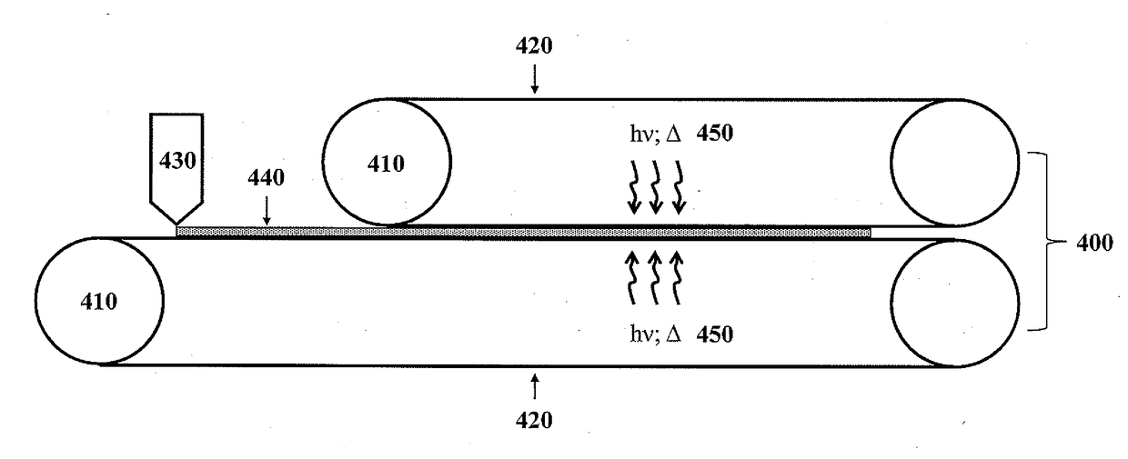
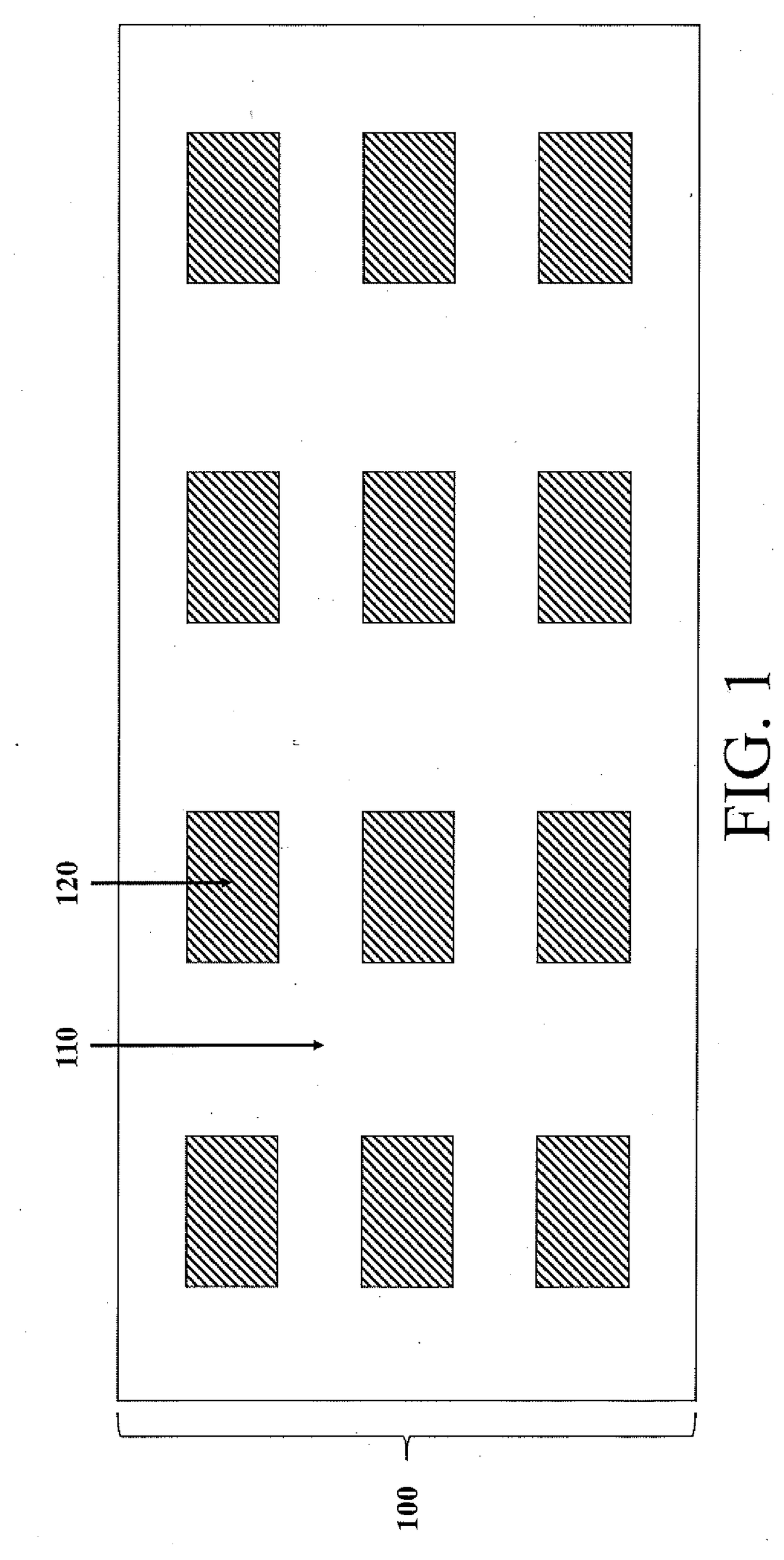
[0039]A stock solution of poly(ethylene-co-acrylic acid) in xylene (5 v / v%) was mounted to a slot-die coating tool and processed into a thin-film atop a carrier substrate via the slot-die coating technique. Samples were the baked at 80° C. in an oven with dry nitrogen flow for 12 hours. The final film was spatially-patterned using standard semiconductor lithographic processing. Atop the patterned film, an excess of a 1.0 M NaOH solution was introduced and soaked for 60 minutes at room temperature. The solution is then flushed with deionized water and the remaining mask is removed. The polymer network is now a spatially-anisotropic substrate for flexible electronics fabrication, wherein electronic elements that cannot accommodate significant strains can be processed directly atop the sodium-salt regions and stretchable interconnects can be utilized to connect such elements.

[0040]As used herein, a polymer network may include either a covalently or physically linked material consisting...


PUM

PropertyMeasurementUnit
Young's modulusaaaaaaaaaa
temperatureaaaaaaaaaa

Abstract

A bulk substrate for stretchable electronics. The bulk substrate is manufactured with a process that forms a soft-elastic region of the bulk substrate. The soft-elastic region includes a strain capacity of greater than or equal to 25% and a first Young's modulus below 10% of a maximum local modulus of the bulk substrate. The process also forms a stiff-elastic region of the bulk substrate. The stiff-elastic region includes a strain capacity of less than or equal to 5% and a second Young's modulus greater than 10% of the maximum local modulus of the bulk substrate.

Description

CROSS-REFERENCE TO RELATED APPLICATIONS[0001]This application claims benefit and priority under 35 U.S.C. §119(e) of U.S. Provisional Application No. 62 / 384,514, filed September 7, 2016. This application is also a Continuation-in-Part application of co-pending U.S. Non-Provisional patent application Ser. No. 15 / 494,000, filed Apr. 21, 2017, which claims benefit and priority under 35 U.S.C. §119(e) of U.S. Provisional Application No. 62 / 413,330, filed Oct. 26, 2016, U.S. Provisional Application No. 62 / 339,410, filed May 20, 2016, and U.S. Provisional Application No. 62 / 339,418, filed May 20, 2016, the disclosures of which are incorporated by reference herein in their entirety for all purposes.TECHNICAL FIELD[0002]The present disclosure relates to the use of substrates for stretchable electronics, and, more particularly, to the use of manufactured substrates having a soft-elastic region comprising a strain capacity of greater than 25% and a first Young's modulus below 10% of a maximum...

Claims


Application Information

Patent Timeline
Patent Type & Authority Applications(United States)
IPC IPC(8): H05K1/02H05K1/03H05K3/00
CPCH05K1/0283H05K1/0393H05K3/0014H05K2203/0143H05K2201/0141H05K3/0023H05K3/0055H01L27/1218H05K1/189H05K2201/0187H05K2203/0796H05K2203/095H05K2203/1163H05K2203/1476H05K2203/1545H05K2203/1194H10K77/111
Inventor REIT, RADUARREAGA-SALAS, DAVID
Owner ARES MATERIALS INC
Why Eureka
Try Eureka