Transmission type chip packaging device

A technology of chip packaging and packaging slots, which is applied in the direction of electrical components, semiconductor/solid-state device manufacturing, circuits, etc., can solve problems affecting chip quality, heat dissipation stability, and easy existence of voids, etc., to reduce void content and eliminate voids , the effect of increasing the area of ​​action

Active Publication Date: 2021-11-05
南通鑫晶电子科技有限公司
View PDF4 Cites 3 Cited by
  • Summary
  • Abstract
  • Description
  • Claims
  • Application Information

AI Technical Summary

Problems solved by technology

[0003] In the prior art, when the chip is packaged with epoxy resin, there are likely to be voids in the epoxy resin formed by casting, which will affect its heat dissipation and stability during use, and affect the quality of the chip after packaging

Method used


Image

  • Transmission type chip packaging device
  • Transmission type chip packaging device
  • Transmission type chip packaging device

Examples


Embodiment 1

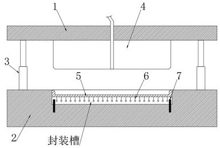
[0043] See figure 1 A chip package transfer means, comprising a fixed platen 2, with a controller mounted on the stationary platen 2, the upper end of the stationary platen 2 by a plurality of cylinders connected to the movable platen 3 with a 1, the lower end of the movable platen 1 is fixedly connected with a pressure module 4, set 2 has an upper end press-cut template module package 4 corresponding to the groove, and the movable platen press 1 through module 4 is fixed to the injection hose, the inner wall of the groove is fixedly connected with a packaging enclosure tray 5, the package and the package tray slot 5 in a space surrounded site there transmitting magnetic indexing module, module pressure plate 4 and a package lower portion opening portion 5 of the chamfer are provided, and both chamfer matched to each other, the effective distance between the control pressure and the chip module 4, to provide a sealing rubber layer Space.

[0044] Further prior art, the disc 5 will...

Embodiment 2

[0052] See Figure 10 Recombinant movable piece cut plurality of through holes respectively corresponding to the moving magnet 832 on the ball 9, fixed to the through hole 11 is connected to the movable piece, the movable piece 11 and the movable magnet 832 is fixedly connected to the ball, the outer magnetic movable secondary ball 831 end fixedly connected to the movable piece 12, movable piece 12 and the upper edge of the movable plate 9 is fixedly connected recombinant, recombinant movable piece 9 of a hard plate-like structure, the movable piece 11 and the movable piece 12 are resilient structure, the electromagnetic tablet 7 is energized, the movable piece 11 at a downwardly deformed at the movable piece 12 upwardly deformed to achieve redistribution of the molten epoxy resin, while when de-energized, the movable plate 12 when the deformation recovery magnetomotive secondary ball 831 generating a hard collision recombinant movable plate 9, so that a certain shock forces, on th...


PUM


Abstract

The invention discloses a transmission type chip packaging device, and belongs to the field of chip packaging. The transmission type chip packaging device is characterized in that two electromagnetic plates are controlled to be powered on and powered off after molten epoxy resin is injected through arrangement of opposite control change ropes and a transmission magnetic guide module, the opposite control change ropes are gradually subjected to downward attraction force in the direction away from the electrified electromagnetic plates, downward pulling force is generated on recombination moving pieces, the recombination moving pieces are deformed towards a glue sealing layer, wave type extrusion force is generated on the glue sealing layer, internal gaps collapse, the molten epoxy resin is forced to be redistributed, and the gaps are effectively eliminated. Compared with the prior art, the chip packaging device has the advantages that the content of gaps in the glue sealing layer after curing is greatly reduced, and the heat dissipation performance of a chip after glue sealing and the use stability of the chip are effectively guaranteed.

Description

Technical field [0001] The present invention relates to the field of chip packages, and more particularly to a transfer chip package device. Background technique [0002] The package can also be said to refer to the outer casing for installing a semiconductor integrated circuit chip, which not only plays, fixes, seals, protects the chip and enhancing thermal conductivity, but also the bridge of the internal world and external circuits - chip The contacts are connected to the pins of the package housing with a wire, which is connected to other devices through the wires on the printed circuit board. Therefore, packaging techniques are very critical for many integrated circuit products. [0003] In the prior art, when the chip is encapsulated by the epoxy resin, the content of the cast-formed epoxy resin is easily void, resulting in the heat dissipationability and the stability of the use, affect the quality of the chip package. Inventive content [0004] 1. Technical issues to be ...

Claims


Application Information

Patent Timeline
Patent Type & Authority Applications(China)
IPC IPC(8): B29C39/10B29C39/22B29C39/24B29C39/26H01L21/56
CPCB29C39/10B29C39/22B29C39/24B29C39/26H01L21/56
Inventor 吴斌
Owner 南通鑫晶电子科技有限公司
Why Eureka
Try Eureka