
A nano-electroplating ultrafast laser intensification and in-situ online monitoring device

An ultrafast laser and monitoring device technology, applied in measuring devices, color/spectral characteristic measurement, electrolytic components, etc., can solve problems such as in-situ online monitoring of laser plating

Active Publication Date: 2022-07-19
WUHAN UNIV
View PDF10 Cites 0 Cited by
  • Summary
  • Abstract
  • Description
  • Claims
  • Application Information

AI Technical Summary

Problems solved by technology

[0004] The present invention solves the problem that laser electroplating cannot be effectively monitored on-line in situ in the prior art by providing an ultra-fast laser strengthening and in-situ online monitoring device for nano-plating

Method used


Image

  • A nano-electroplating ultrafast laser intensification and in-situ online monitoring device
  • A nano-electroplating ultrafast laser intensification and in-situ online monitoring device

Examples


Embodiment Construction

[0028] In order to better understand the above technical solutions, the above technical solutions will be described in detail below with reference to the accompanying drawings and specific embodiments.

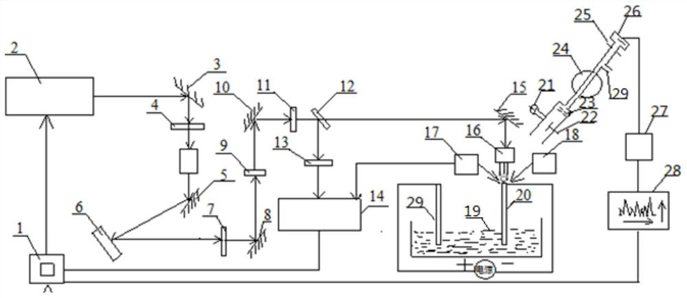
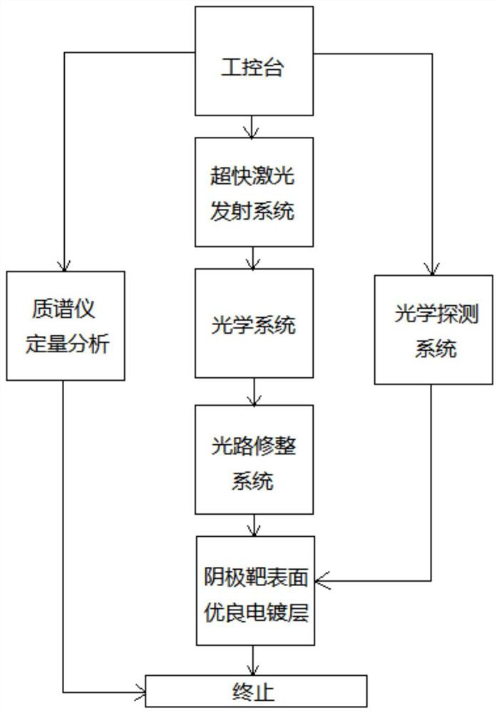
[0029] This embodiment provides a nano-electroplating ultrafast laser enhancement and in-situ online monitoring device, see figure 1 , figure 2 , mainly including: industrial console 1, ultrafast laser 2, spectrometer 14, laser probe 16, holographic camera 17, pulse generator 18, mass spectrometer and optical path system.

[0030] The pulse electroplating power supply is respectively connected with the anode 29 and the micro-nano device cathode target 20 placed in the electroplating pool 19, and the micro-nano device cathode target 20 is the object of nano-electroplating processing; the laser probe 16, the holographic camera 17 and The pulse generators 18 are all arranged in the vicinity of the cathode target 20 of the micro-nano device. The industrial computer 1 is respect...


PUM

PropertyMeasurementUnit
wavelengthaaaaaaaaaa

Abstract

The invention belongs to the technical field of micro-nano device manufacturing, and discloses a nano-electroplating ultrafast laser intensification and in-situ online monitoring device, comprising an industrial console, an ultrafast laser, a spectrometer, a laser probe, a holographic camera, a pulse generator, a mass spectrometer and a Optical path system; laser probe, holographic camera and pulse generator are all arranged in the vicinity of the cathode target of micro-nano device; industrial computer is respectively connected with ultrafast laser, spectrometer, pulse generator, mass spectrometer and pulse electroplating power supply; holographic camera is connected with Spectrometer connection. The invention can perform in-situ on-line monitoring of laser electroplating.

Description

technical field [0001] The invention belongs to the technical field of micro-nano device manufacturing, and more particularly relates to a nano-electroplating ultrafast laser intensification and in-situ online monitoring device. Background technique [0002] With the rapid development of the computer and microelectronic instrumentation industries, the demand for microelectronic components and large-scale integrated circuit boards has surged. Gold plating has been widely used in the above industries for its excellent properties such as high heat resistance, high electrical conductivity and easy soldering. In this field, the traditional gold plating production process is to use the method of mask re-plating or full plating and then etching. These processes are not only time-consuming, but also waste a lot of expensive gold. People have been looking for a more economical gold plating technology, so laser-enhanced gold plating came into being. [0003] Compared with the tradi...

Claims


Application Information

Patent Timeline
Patent Type & Authority Patents(China)
IPC IPC(8): C25D17/00C25D21/12C21D10/00C22F3/00C25D5/02G01N21/25G01N27/62
CPCC25D17/00C25D21/12C25D5/024C21D10/005C22F3/00G01N27/62G01N21/25
Inventor 刘胜周振东芳
Owner WUHAN UNIV
Learn More