Semiconductor wafer corrosion device

A technology for etching devices and wafers, which is used in the manufacture of semiconductor/solid-state devices, cleaning flexible items, electrical components, etc. Removes the effect of uniform thickness

Active Publication Date: 2021-11-05
南通西瑞电子科技有限公司
View PDF7 Cites 4 Cited by
  • Summary
  • Abstract
  • Description
  • Claims
  • Application Information

AI Technical Summary

Problems solved by technology

[0006] Aiming at the deficiencies of the prior art, the present invention provides a semiconductor wafer etching device, which has the advantages of uniform removal thickness of the damaged layer, consistent etching time of each wafer, repeated use of etching liquid and cleaning liquid, etc., and solves the problem of etching liquid and cleaning liquid. The problem that the cleaning solution cannot be used multiple times and the thickness of the damaged wafer layer is removed uniformly

Method used


Image

  • Semiconductor wafer corrosion device
  • Semiconductor wafer corrosion device
  • Semiconductor wafer corrosion device

Examples


Embodiment Construction

[0034] The following will clearly and completely describe the technical solutions in the embodiments of the present invention with reference to the accompanying drawings in the embodiments of the present invention. Obviously, the described embodiments are only some, not all, embodiments of the present invention. Based on the embodiments of the present invention, all other embodiments obtained by persons of ordinary skill in the art without making creative efforts belong to the protection scope of the present invention.

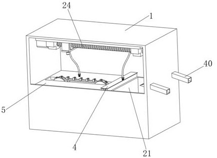
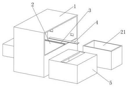
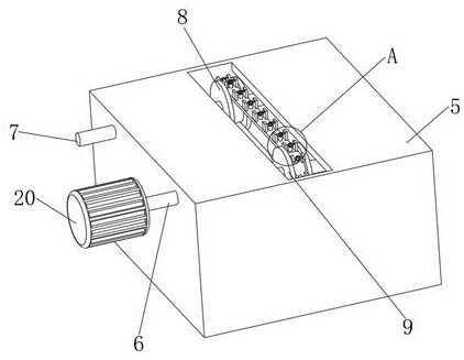
[0035] see Figure 1-9, a semiconductor wafer etching device, the device includes a casing 1, a partition 2 is fixedly arranged in the casing 1, a slot 3 is opened on the top of the partition 2, and a block 4 is clipped in the slot 3, and the block 4 The upper part is provided with a sponge, which is used to absorb the corrosion liquid dripped during the movement of the wafer, so as to prevent the corrosion liquid from falling inside the shell 1 and damaging t...


PUM


Abstract

The invention discloses a semiconductor wafer corrosion device. The semiconductor wafer corrosion device comprises a shell, a corrosion liquid box and a cleaning box are arranged in the shell, wherein corrosion liquid and cleaning liquid are contained in the corrosion liquid box and the cleaning box respectively, a rotating mechanism is arranged in the corrosion liquid box, and the rotating mechanism is arranged on the liquid level of the corrosion liquid in a penetrating mode; and a clamping moving mechanism is arranged on an upper portion in the shell, and the clamping moving mechanism is used for clamping the corroded wafer and then moving the wafer into the cleaning box to be cleaned. According to the semiconductor wafer corrosion device, a balance module is arranged in the rotating mechanism, so a lower surface of the wafer clamped in the elastic block is integrally in contact with the liquid level of the corrosive liquid in the process of entering the corrosive liquid, the time difference of the same plane entering the corrosive liquid in the process of entering the corrosive liquid of the wafer is avoided, and uniform removal thickness of a damaged layer is ensured.

Description

technical field [0001] The invention relates to the technical field of wafer etching, in particular to a semiconductor wafer etching device. Background technique [0002] Wafer refers to the silicon wafer used in the production of silicon semiconductor integrated circuits. Because of its circular shape, it is called a wafer. After the semiconductor silicon wafer is thinned and ground, there is a layer of mechanical damage on the surface of the silicon wafer, mainly silicon. Before polishing, it must be removed. At present, alkaline solution is used for removal. The uniformity of the thickness of the corrosion damage layer directly affects the TTV and physical and chemical test results in the geometric parameters, and even affects the production of the subsequent process. [0003] The Chinese invention patent number is CN201510420064.1, which discloses a large-size grinding wafer surface corrosion device, including: feet, recovery tanks, suction cup brackets, suction cups, an...

Claims


Application Information

Patent Timeline
Patent Type & Authority Applications(China)
IPC IPC(8): H01L21/67B08B11/00
Inventor 蔡守波
Owner 南通西瑞电子科技有限公司
Why Eureka
Try Eureka