Photon neural network chip

A neural network and photonic technology, applied in the field of photonic neural network chips, can solve the problems of complex chips, affecting the calculation accuracy, and the large number of cascades of photon term shifters, and achieve the effect of high energy efficiency ratio advantage.

Pending Publication Date: 2021-11-09
光子算数(苏州)智能科技有限公司
View PDF0 Cites 2 Cited by
  • Summary
  • Abstract
  • Description
  • Claims
  • Application Information

AI Technical Summary

Problems solved by technology

However, the disadvantage of this method is also obvious. When the required calculation is more complicated, the chip realized by this method will be very complicated, and the number of cascaded photon shifters will be very large, which will affect the final calculation accuracy.

Method used


Image

  • Photon neural network chip

Examples


Embodiment

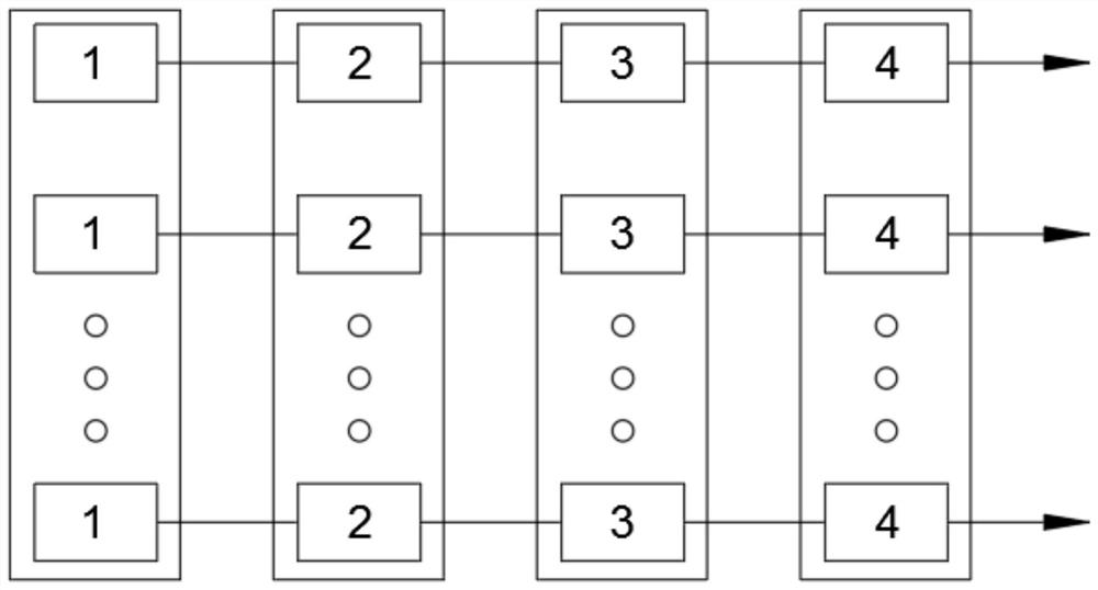
[0015] Embodiment: a kind of photonic neural network chip, such as figure 1 As shown, it includes a laser source array 1, a wavelength division multiplexer array 2, a photon convolution kernel array 3 and an optical microring resonator array 4, and the laser source array has several output terminals in total, and the wavelength division multiplexer array Consisting of several input terminals, several wavelength division multiplexers and several output terminals, the photon convolution kernel array includes several photon convolution kernels of the same structure, and the optical microring resonator array includes several optical microring resonator.

[0016] The nth output end of the laser source array is connected to the nth input end of the wavelength division multiplexer array, and the nth output end of the wavelength division multiplexer array is connected to the nth output end of the photon convolution kernel array. The input ends are connected, and the output end of the...


PUM


Abstract

The present invention discloses a photon neural network chip which comprises a laser source array, a wavelength division multiplexer array, a photon convolution kernel array and an optical micro-ring resonator array, the laser source array is provided with a plurality of output ends, the wavelength division multiplexer array is composed of a plurality of input ends, a plurality of wavelength division multiplexers and a plurality of output ends, the photon convolution kernel array comprises a plurality of photon convolution kernels with the same structure, and the light micro-ring resonator array comprises a plurality of light micro-ring resonators. According to the chip, light is used as a numerical calculation medium, the speed of convolution calculation is increased to a constant level, and meanwhile, the method has the advantage of higher energy efficiency ratio.

Description

technical field [0001] The invention belongs to the technical field of photonic signals, in particular to a photonic neural network chip. Background technique [0002] Photonic integration technology uses light as the carrier of transmission and processing, which can easily break through the bandwidth bottleneck of electronic technology and provide strong support for future ultra-large bandwidth and ultra-high-speed computing. Therefore, using photonic technology to implement a deep learning computing chip, that is, a neural network chip, has become a research hotspot. [0003] The Massachusetts Institute of Technology has developed a photonic neural network chip that can realize matrix multiplication by using coherent optics. However, the disadvantage of this method is also obvious. When the required calculation is more complicated, the chip realized by this method will be very complicated, and the number of cascaded photon phase shifters will be very large, which will aff...

Claims


Application Information

Patent Timeline
Patent Type & Authority Applications(China)
IPC IPC(8): H04J14/02H04B10/516G06N3/063
CPCH04J14/0202H04B10/516G06N3/063
Inventor 白冰
Owner 光子算数(苏州)智能科技有限公司
Why Eureka
Try Eureka