A semiconductor part processing jig

A part processing and semiconductor technology, applied in the field of semiconductor part processing fixtures, can solve the problems of time-consuming work, affecting the quality of semiconductor products, low efficiency, etc., and achieve the effect of improving work efficiency

Active Publication Date: 2021-12-21
南通普祥金属制品有限公司
View PDF8 Cites 0 Cited by
  • Summary
  • Abstract
  • Description
  • Claims
  • Application Information

AI Technical Summary

Problems solved by technology

[0005] The object of the present invention is to provide a semiconductor part processing jig, which solves the need to continuously turn over the semiconductor material in the background technology, but the semiconductor material is small in size and difficult to turn over, resulting in a lot of work time spent in the dispensing process , the efficiency is low, and secondly, in the dispensing process, it is difficult to spread the glue, causing the glue to accumulate together, which leads to the poor effect of the glue and affects the quality of semiconductor products after dispensing

Method used


Image

  • A semiconductor part processing jig
  • A semiconductor part processing jig
  • A semiconductor part processing jig

Examples


Embodiment Construction

[0033] The following will clearly and completely describe the technical solutions in the embodiments of the present invention with reference to the accompanying drawings in the embodiments of the present invention. Obviously, the described embodiments are only some, not all, embodiments of the present invention. Based on the embodiments of the present invention, all other embodiments obtained by persons of ordinary skill in the art without making creative efforts belong to the protection scope of the present invention.

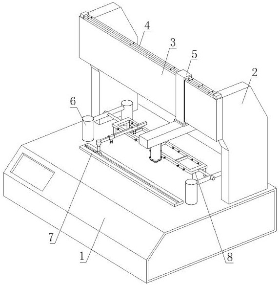
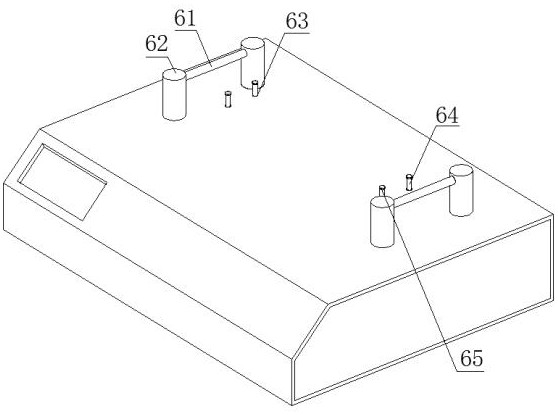
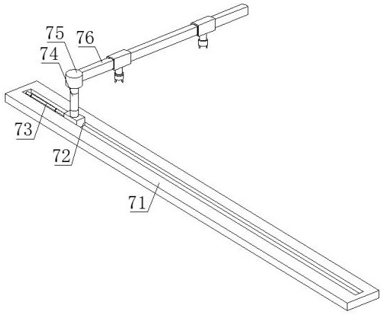
[0034] refer to figure 1 , a semiconductor parts processing fixture, including a processing table 1, a vertical plate 2 arranged on the upper surface of the processing table 1, a horizontal plate 3 arranged on one side of the vertical plate 2, and a push assembly 4 arranged on the upper end of the horizontal plate 3, The outer surface of the horizontal plate 3 is provided with a rubber extruding mechanism 5, the upper surface of the processing table 1 is provi...


PUM


Abstract

The invention relates to the technical field of semiconductor processing equipment, and discloses a semiconductor part processing jig, including a processing table, a vertical plate arranged on the upper surface of the processing table, a horizontal plate arranged on one side of the vertical plate, and a vertical plate arranged on the top of the horizontal plate Pushing the assembly, the outer surface of the horizontal plate is provided with a rubber extruding mechanism, the upper surface of the processing table is provided with an auxiliary mechanism and an external connection mechanism, and the upper surface of the processing table is provided with a placement mechanism, and the semiconductor product is placed inside the placement groove. After completing a After facing, rotate the rotating rod to make the placing plate rotate one circle. While rotating, the electromagnetic plate A and electromagnetic plate B are brought with opposite magnetism, so that the inner plate moves down, and the inner rod moves down accordingly. After the rotation, the electromagnetic plate Board A and electromagnetic board B have the same magnetism, the inner rod moves up, the magnetic suction board and the placement board are magnetically connected, and the support for the placement board is completed again, which is convenient for the subsequent dispensing process. The whole process does not need to be turned over manually, which improves efficiency. It also reduces the traces left by manual contact by staff.

Description

technical field [0001] The invention relates to the technical field of semiconductor processing equipment, in particular to a jig for processing semiconductor parts. Background technique [0002] Semiconductors refer to materials whose conductivity is between conductors and insulators at room temperature. Semiconductors are used in integrated circuits, consumer electronics, communication systems, photovoltaic power generation, lighting, high-power power conversion and other fields. For example, diodes are devices made of semiconductors. At the same time, the fixture is a large class of tools for woodworking, ironwork, fitter, machinery, electric control and other handicrafts, mainly as a tool to assist in controlling position or movement (or both). Fixtures can be divided into process assembly fixtures, project test fixtures and circuit board test fixtures. In the semiconductor field, dispensing fixtures are indispensable. [0003] The current dispensing processing jig need...

Claims


Application Information

Patent Timeline
Patent Type & Authority Patents(China)
IPC IPC(8): B05C13/02B05C5/02B05C11/02B05C11/10
CPCB05C13/02B05C5/0208B05C11/023B05C11/1039
Inventor 何峰
Owner 南通普祥金属制品有限公司
Why Eureka
Try Eureka