Semiconductor equipment and purging method

A semiconductor and equipment technology, applied in the field of semiconductor equipment and purging, can solve the problems affecting the detection effect and service life of sensors

Pending Publication Date: 2021-12-14
CHANGXIN MEMORY TECH INC
View PDF0 Cites 0 Cited by
  • Summary
  • Abstract
  • Description
  • Claims
  • Application Information

AI Technical Summary

Problems solved by technology

[0004] The application provides a semiconductor device and a purging method to solve the problem that the inside

Method used


Image

  • Semiconductor equipment and purging method
  • Semiconductor equipment and purging method
  • Semiconductor equipment and purging method

Examples


Embodiment Construction

[0048] In order to make the purpose, technical solutions and advantages of this application clearer, the technical solutions in this application will be clearly and completely described below in conjunction with the accompanying drawings in this application. Obviously, the described embodiments are part of the embodiments of this application , but not all examples. Based on the embodiments in this application, all other embodiments obtained by persons of ordinary skill in the art without making creative efforts belong to the scope of protection of this application.

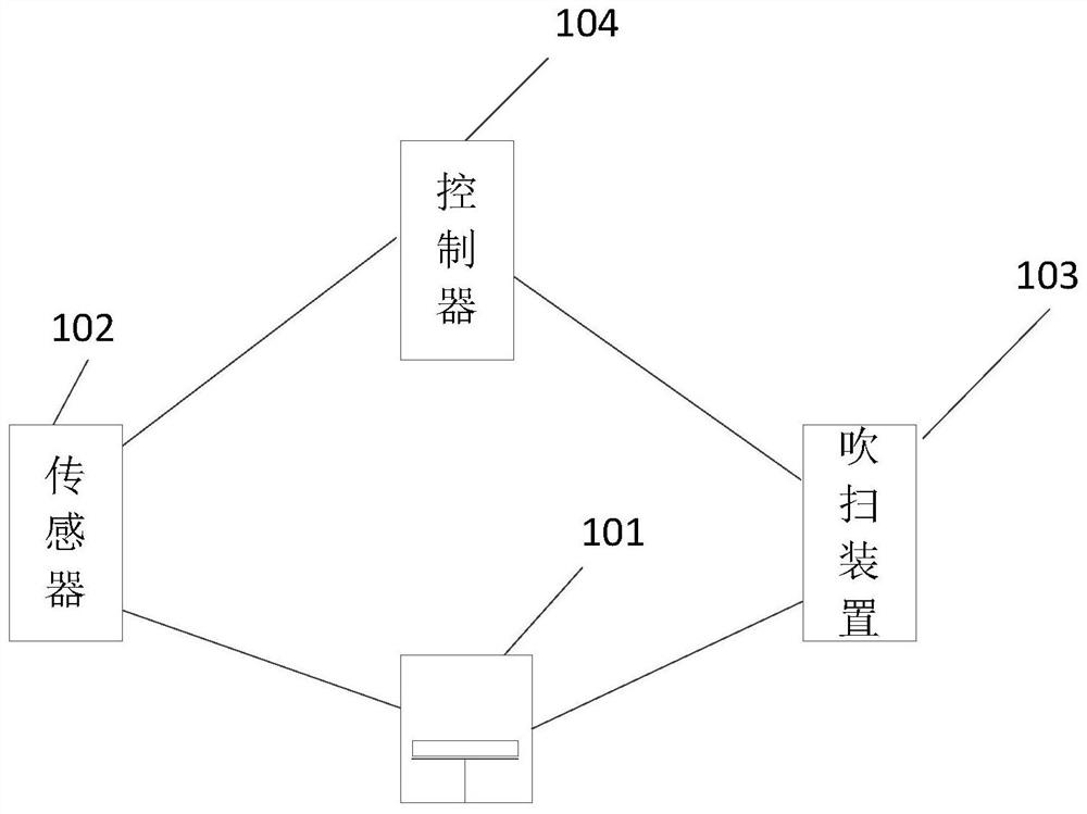
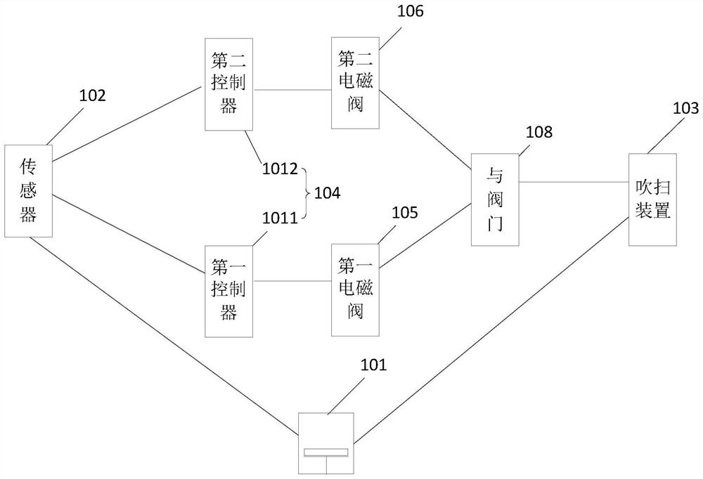
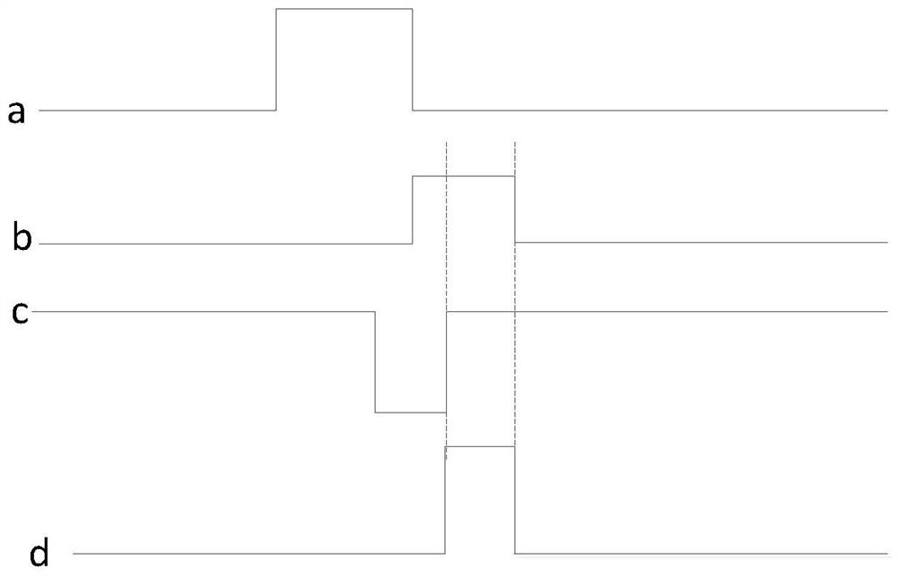
[0049] Processing equipment in the semiconductor field, such as chemical mechanical polishing (CMP) machines, wet process (Wet) machines, thin film processing (thin film) machines, usually use sensors to detect the reaction chambers (chambers) of various machines Whether there is a wafer, for example, using a fiber optic sensor to detect whether there is a wafer in the reaction chamber. When there is a wafer in t...


PUM


Abstract

The invention provides semiconductor equipment and a purging method. The semiconductor equipment comprises a reaction chamber, a sensor, a purging device and a controller, and the controller is connected with the sensor and the purging device. The sensor detects whether a wafer exists in the reaction chamber or not and sends a detection signal to the controller, the controller generates a purging signal according to the detection signal and sends the detection signal and the purging signal to the purging device, and the purging device purges the sensor after receiving the detection signal and the purging signal so as to remove water drops attached to the sensor due to a wet environment, so light intensity loss caused by the water drops is reduced, the service life of the sensor is prolonged, reflection or refraction caused by the water drops is reduced, the detection effect of the sensor is improved, the semiconductor equipment can normally process wafers, and the yield of the wafers is improved.

Description

technical field [0001] The present application relates to the technical field of semiconductors, in particular to a semiconductor device and a purging method. Background technique [0002] Existing semiconductor machines usually use sensors to detect whether there is a wafer in the reaction chamber. If there is a wafer in the reaction chamber, the wafer will be processed. The circle is transferred into the reaction chamber. [0003] However, when water, chemical liquids, compounds, etc. exist in the reaction chamber, the interior of the reaction chamber is a humid environment, which affects the detection effect and service life of the sensor. Contents of the invention [0004] The present application provides a semiconductor device and a purging method, which are used to solve the problem that the inside of the reaction chamber is a humid environment, which affects the detection effect and service life of the sensor. [0005] In a first aspect, the present application pr...

Claims


Application Information

Patent Timeline
IPC IPC(8): H01L21/67F26B21/00
CPCH01L21/67265F26B21/004
Inventor 何家平
Owner CHANGXIN MEMORY TECH INC
Why Eureka
Try Eureka