Memory cell array of programmable non-volatile memory
A storage unit array and storage unit technology, applied in static memory, read-only memory, digital memory information, etc., can solve the problem of large size
- Summary
- Abstract
- Description
- Claims
- Application Information
AI Technical Summary
Problems solved by technology
Method used
Image

Examples
Embodiment Construction
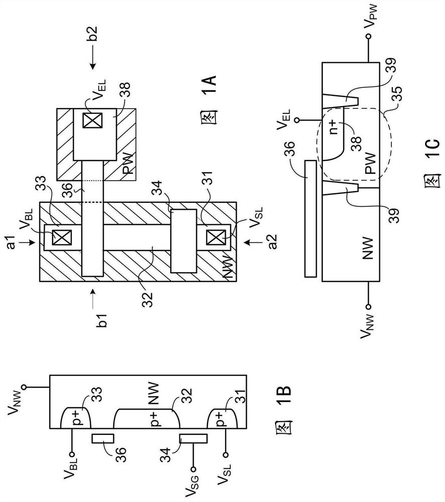
[0037] Figures 2A to 2E Production process programmable non-volatile memory of the present invention. According to an embodiment of the present invention, non-volatile memory can be programmed once (OTP) non-volatile memory, erasable or repeatedly programming (MTP) non-volatile memory. Further, in this production process, a memory cell is described the production process, but the present invention is not limited thereto.
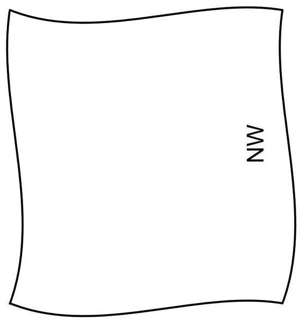
[0038] First of all, if Figure 2A Shown, an N-type well region (N-well region, NW) on a semiconductor substrate (substrate). Wherein the semiconductor substrate may be a p-type semiconductor substrate (p-substrate).
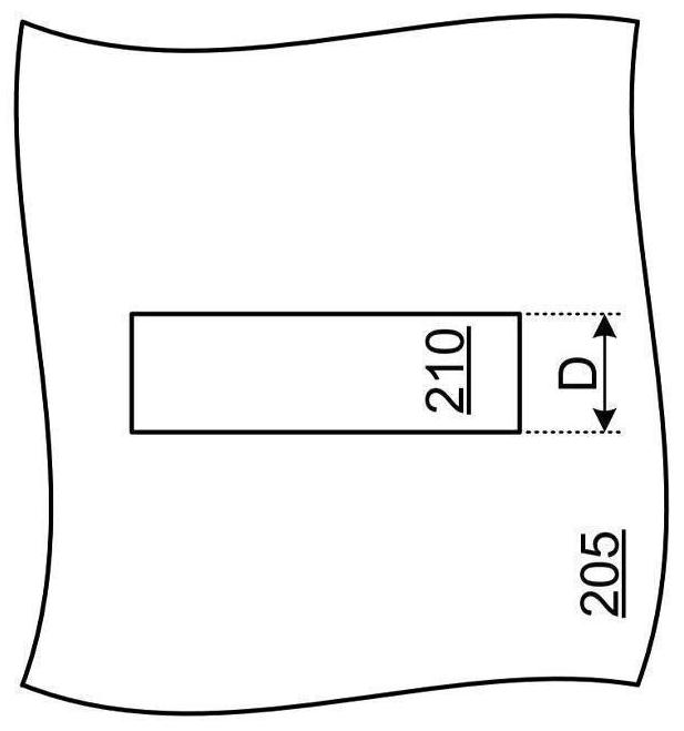
[0039] Next, the isolation structure (isolation structure) forming step. like Figure 2b , In the semiconductor substrate (not shown), N-type well region NW surfaces defining a width D of a rectangular area 210. Subsequently, an outer rectangular region 210 in the isolation structure 205 is formed, to retain only the surface of the N-type well regi...
PUM
 Abstract
Description
Claims
Application Information
 - R&D
- Intellectual Property
- Life Sciences
- Materials
- Tech Scout
- Unparalleled Data Quality
- Higher Quality Content
- 60% Fewer Hallucinations
Browse by: Latest US Patents, China's latest patents, Technical Efficacy Thesaurus, Application Domain, Technology Topic, Popular Technical Reports.
© 2025 PatSnap. All rights reserved.Legal|Privacy policy|Modern Slavery Act Transparency Statement|Sitemap|About US| Contact US: help@patsnap.com