Electroluminescent semiconductor plate surface defect AI detection method

A detection method and semiconductor technology, applied in material defect testing, neural learning methods, image analysis, etc., can solve the problems of small pixel algorithm network, lack of accurate defect positioning, slow recognition process, etc., to improve generalization ability, The effect of improving recognition accuracy and recognition speed and increasing model complexity

Pending Publication Date: 2021-12-21
陈博源
View PDF2 Cites 1 Cited by
  • Summary
  • Abstract
  • Description
  • Claims
  • Application Information

AI Technical Summary

Problems solved by technology

[0006] Aiming at the deficiencies of the prior art, the present invention aims to provide an AI detection method for surface defects of electroluminescent semiconductor plates, in order to solve the problem of single image data, small pixel algorithm network scale, slow recognition process speed and low accuracy in the prior art. Lack of technical issues with accurate positioning of defects

Method used


Image

  • Electroluminescent semiconductor plate surface defect AI detection method
  • Electroluminescent semiconductor plate surface defect AI detection method
  • Electroluminescent semiconductor plate surface defect AI detection method

Examples


Embodiment

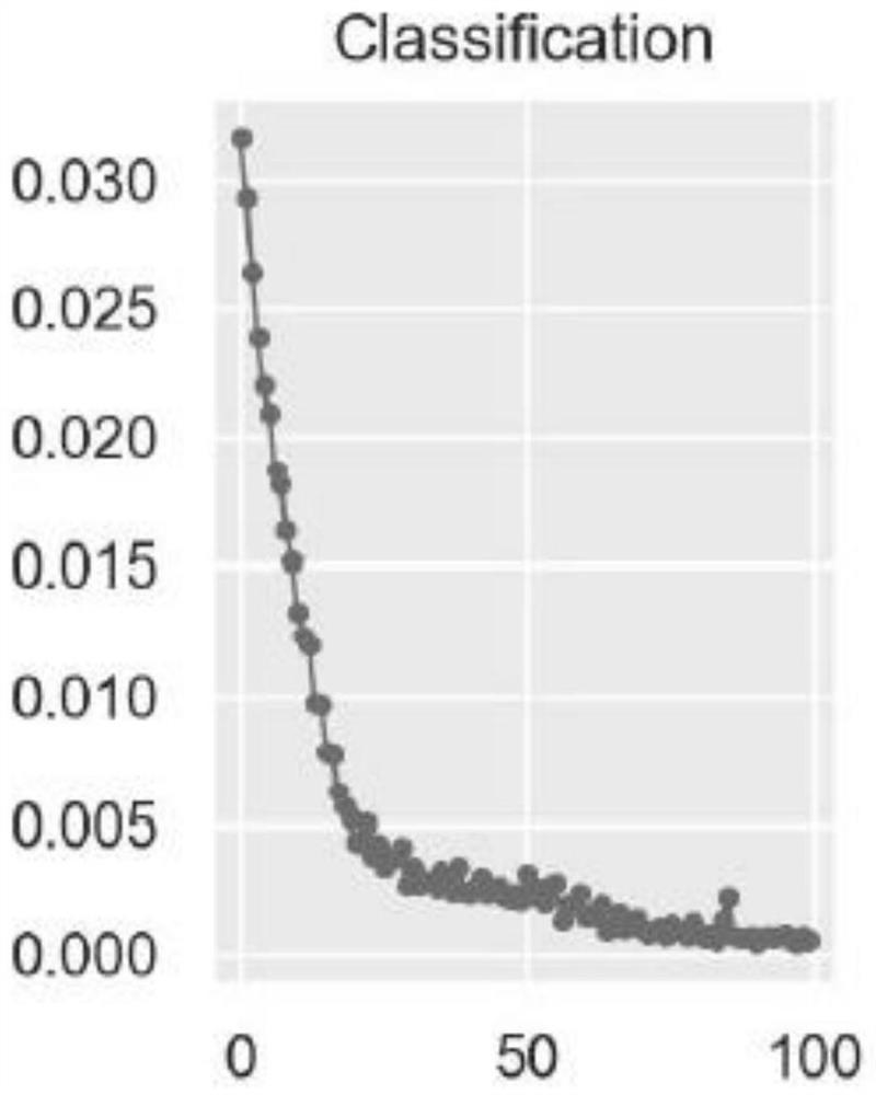
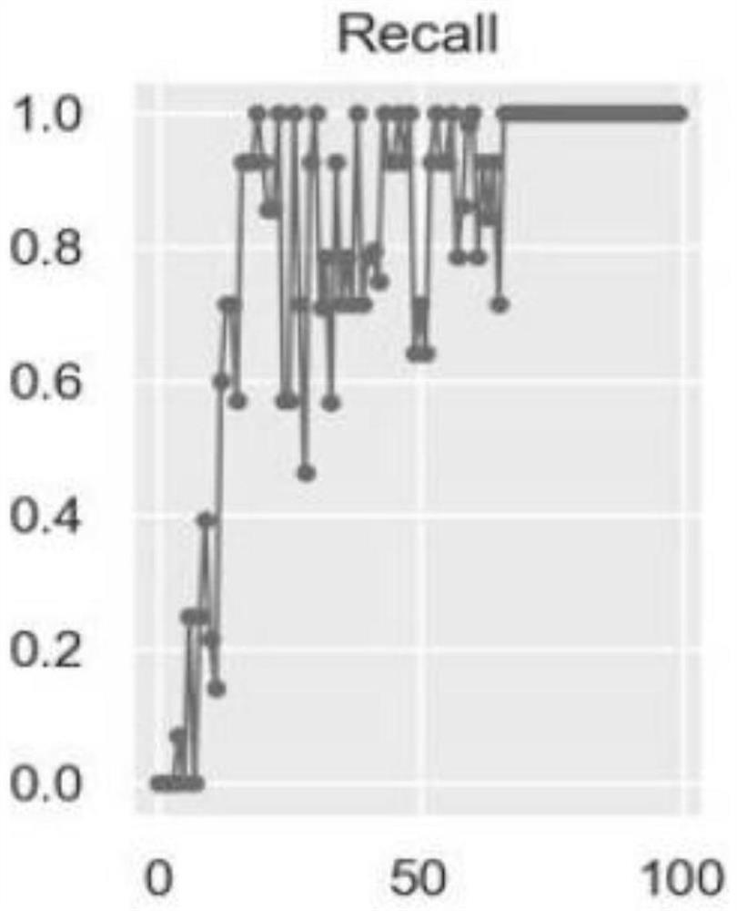
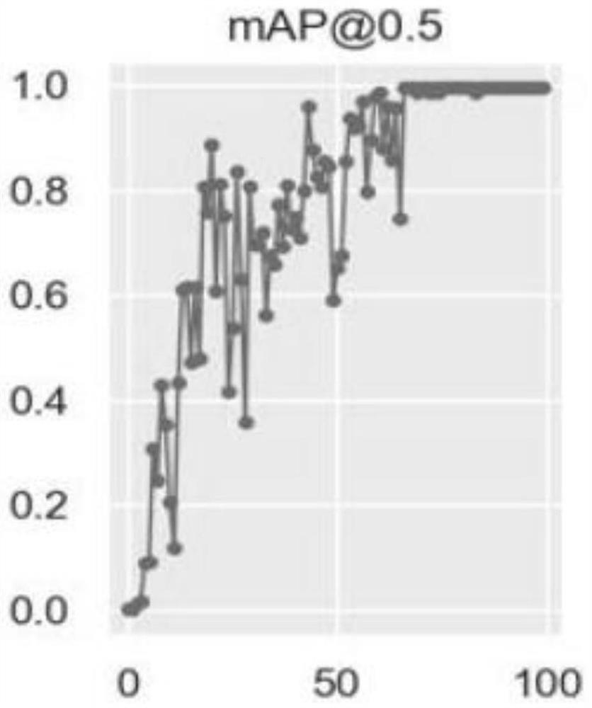
[0052] Electroluminescent technology is used to take pictures on the surface of the silicon carbide semiconductor flat plate, and then the defect detection is carried out by the method of the present invention, and the detection steps are as follows:

[0053] Electroluminescent technology is used to take pictures on the surface of silicon semiconductor photovoltaic modules, and then carry out defect detection by the method of the present invention. The detection steps are as follows:

[0054] 1. Carry out the first image enhancement processing

[0055] (1) Input 500 electroluminescent images of semiconductor plates containing black spots and cracks, and use the image cropping function to adjust the pixel size of the input image to a square image of 640×640;

[0056] (2) Design an image random flip algorithm, and set the flip probability of the image in the horizontal direction and vertical direction to 0.5. Perform image flipping and save;

[0057] (3) Design an image random r...


PUM


Abstract

The invention relates to an electroluminescent semiconductor plate surface defect AI detection method. The method comprises the steps of carrying out first image enhancement processing, carrying out image defect labeling and conversion, training random distribution of verification test images, carrying out second image enhancement processing, establishing a target detection neural network, carrying out data training to obtain optimal weight parameters, and carrying out plate image AI detection. The objective of the invention is to solve the problems of low defect identification speed, low accuracy and lack of accurate classification and positioning capability due to limitation of quality and quantity of image data sets, single image data preprocessing method and small pixel algorithm network scale when defect detection is carried out on the surface of an electroluminescent semiconductor plate in the prior art. The method is suitable for detecting semiconductor chips and panels such as silicon, germanium, gallium arsenide and silicon carbide.

Description

technical field [0001] The invention relates to an AI detection method for surface defects, in particular to an AI detection method for surface defects of electroluminescent semiconductor plates, belonging to the fields of image recognition and nondestructive testing. Background technique [0002] Electroluminescence (English electroluminescent) is referred to as EL. EL detection is a testing technology that uses near-infrared images taken by high-resolution infrared cameras to detect surface defects on boards. It plays a key role in the fields of photovoltaic power station operation and maintenance. Among them, EL images The identification of defect feature information is the core part of the detection process. [0003] Chinese patent 201810794758.5 ​​discloses a solar cell electroluminescence image detection and defect identification method, which specifically includes the following steps: obtaining the solar cell electroluminescence image to be detected, positioning the g...

Claims


Application Information

Patent Timeline
Patent Type & Authority Applications(China)
IPC IPC(8): G06T7/00G06T5/00G01N25/72G06N3/04G06N3/08
CPCG06T7/0004G06T5/009G06N3/08G01N25/72G06T2207/10004G06T2207/20081G06T2207/20084G06T2207/30148G06N3/045G06T2207/10048G06T2207/30164
Inventor 陈博源
Owner 陈博源
Why Eureka
Try Eureka