Automatic chip alignment device and alignment method

An automatic alignment and chip technology, which is applied in the direction of measuring devices, instruments, electronic circuit testing, etc., can solve the problems of poor surface flatness of the test bench, the influence of chip test results, and the impact of chip conductivity and thermal conductivity, etc., to achieve electrical conductivity It has the effect of stabilizing thermal conductivity, improving test accuracy and ensuring accuracy

Active Publication Date: 2022-02-18
HEBEI KTHAHCO TECH CO LTD
View PDF0 Cites 0 Cited by
  • Summary
  • Abstract
  • Description
  • Claims
  • Application Information

AI Technical Summary

Problems solved by technology

[0004] Therefore, the technical problem to be solved by the present invention is to overcome the possible displacement and angular deflection of the chip when the chip is placed on the slide table in the prior art. Inaccuracy will affect the test results of the chip, making the quality of the chip uneven; on the other hand, the random placement of the chip makes the surface of the test bench wear inconsistent. After a period of use, the surface flatness of the test bench is poor, making the chip and test Inhomogeneous surface contact of the stage affects the stringent requirements of the chip for electrical and thermal conductivity
Thereby providing an automatic chip alignment device and alignment method

Method used


Image

  • Automatic chip alignment device and alignment method
  • Automatic chip alignment device and alignment method
  • Automatic chip alignment device and alignment method

Examples


Embodiment 1

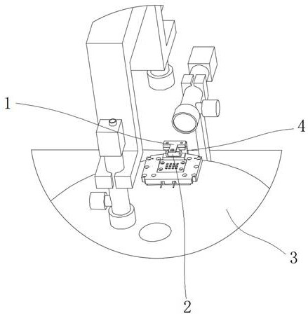
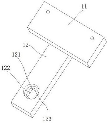
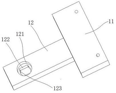
[0040] This embodiment provides a specific implementation of the chip automatic alignment device, such as figure 1 , figure 2 , image 3 and Figure 4 As shown, the alignment member 1 is installed on the moving mechanism 4, and the moving mechanism 4 can drive the alignment member 1 to move in the first direction and / or the second direction above the plane where the slide table 2 is located. The second directions are perpendicular to each other, wherein the plane where the slide table 2 is located is the plane where chips are placed on the slide table 2 , and the plane where the alignment member 1 moves is parallel to the plane where the slide table 2 is located. The alignment member 1 has a correction plate 12, which is set correspondingly to the slide table 2. The correction plate 12 is set above the slide table 2. A first hole 122 is opened on the correction plate 12, and the chip can pass through the first hole 122. The holes 122 drop onto the slide table 2; a group of...

Embodiment 2

[0055] This embodiment provides a specific implementation of the alignment method, which is implemented by using the chip automatic alignment device in Example 1, including the following steps: placing the chip on the loading table 2, and the calibration plate 12 pushes the chip on the loading table. The chip stage 2 is moved along the first direction and / or the second direction until it reaches a predetermined position, and the luminous point of the chip corresponds to and does not touch the escape groove 123 on the calibration plate 12 during the movement; wherein, the first direction and The second directions are perpendicular to each other.

[0056] The calibration plate 12 is controlled by the moving mechanism 4 to push the chip to move along the first direction and the second direction on the slide table 2. During the movement, the light-emitting point on the chip is in the avoidance groove 123; during the movement, it passes through the first hole. Body 122 adjusts the ...


PUM


Abstract

The invention provides an automatic chip alignment device and an alignment method, which belong to the technical field of laser chip detection equipment. The chip automatic alignment device includes: a moving mechanism; an alignment piece, and the alignment piece has a correction plate; The first hole body is suitable for the chip to pass through, and a group of opposite sides of the first hole body is provided with avoidance grooves. The chip automatic alignment device provided by the present invention drives the alignment member to move forward, backward, left, and right in the first direction and the second direction by controlling the moving mechanism. The chip is adjusted in angle and position under the action of the side of the first hole, and an avoidance groove is provided on the first hole, and the avoidance groove can prevent the light-emitting point on the chip from touching the side of the first hole. Ensure that the chip is in an accurate position and angle during detection, avoid the phenomenon that the detection mechanism cannot accurately detect the corresponding position on the chip, and ensure the accuracy of the chip detection result.

Description

technical field [0001] The invention relates to the technical field of laser chip detection equipment, in particular to an automatic chip alignment device and alignment method. Background technique [0002] An integrated circuit (Integrated Circuit, IC), also known as a microchip, chip or chip, is a way of miniaturizing circuits (including semiconductor devices, including passive components, etc.), and is often manufactured on the surface of a semiconductor wafer. [0003] With the development of the semiconductor industry, the thickness of integrated circuit chips is becoming thinner and thinner, and the processing and detection accuracy of chips is getting higher and higher. For the chip size manufactured by the manufacturer, the most common size is a rectangle. After the existing chip is processed, it needs to be tested by a testing agency to ensure the quality and performance of the chip. The existing testing method is usually to use a suction nozzle to place the chip on...

Claims


Application Information

Patent Timeline
Patent Type & Authority Patents(China)
IPC IPC(8): G01R31/28H01L21/68
CPCG01R31/2891G01R31/2893H01L21/68H01L21/681
Inventor 杜海洋牛超凡赵莉娜梁书尧张明亮刘强
Owner HEBEI KTHAHCO TECH CO LTD
Why Eureka
Try Eureka