A kind of selective passivation contact structure of solar cell and double-sided solar cell

A solar cell and contact structure technology, applied in the field of solar cells, to achieve the effects of improving short-circuit current, good interface passivation performance, and low contact resistance

Active Publication Date: 2022-02-11
ZHEJIANG AIKO SOLAR ENERGY TECH CO LTD
View PDF0 Cites 0 Cited by
  • Summary
  • Abstract
  • Description
  • Claims
  • Application Information

AI Technical Summary

Problems solved by technology

[0005] The embodiment of the present application provides a selective passivation contact structure of solar cells and double-sided solar cells, aiming to solve the problem of how to reduce the parasitic absorption of solar cells

Method used


Image

  • A kind of selective passivation contact structure of solar cell and double-sided solar cell
  • A kind of selective passivation contact structure of solar cell and double-sided solar cell
  • A kind of selective passivation contact structure of solar cell and double-sided solar cell

Examples


Embodiment 1

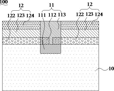
[0035] Embodiment 1 of the present application provides a selective passivation contact structure of a solar cell. For convenience of description, only parts related to the embodiment of the present application are shown.

[0036] see figure 1 The selective passivation contact structure 100 of the solar cell provided by the embodiment of the present application includes: first passivation contact regions 11 and second passivation contact regions 12 arranged alternately; The first doped layer 111, the first passivation layer 112 and the second doped layer 113 on the silicon substrate 10; the second passivation contact region 12 includes the second passivation layer stacked on the silicon substrate 10 in sequence 122, the third doped layer 123 and the third passivation layer 124; the thickness of the second doped layer 113 is greater than the thickness of the third doped layer 123, the doping of the second doped layer 113 and the third doped layer 123 same polarity.

[0037] ...

Embodiment 2

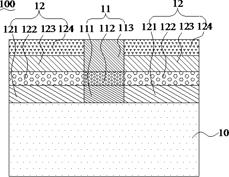
[0078] see Figure 5 , Embodiment 2 of the present application also provides a double-sided solar cell 1000, the double-sided solar cell 1000 includes a silicon substrate 10, the selective passivation contact structure 100 of Embodiment 1, and a first conductive layer 30, the selective passivation The contact structure 100 is disposed on one side of the silicon substrate 10 , and the second doped layer 113 is connected to the first conductive layer 30 .

[0079] In the double-sided solar cell 1000 of the second embodiment of the present application, since the thickness of the third doped layer 123 is small, the parasitic absorption of the second passivation contact region 12 can be reduced and the short-circuit current can be increased. At the same time, since the second doped layer 113 is thicker, it can prevent the first conductive layer 30 from burning through the second doped layer 113 and increase the open circuit voltage. At the same time, it can have excellent interfac...


PUM

PropertyMeasurementUnit
pore sizeaaaaaaaaaa
thicknessaaaaaaaaaa
thicknessaaaaaaaaaa

Abstract

The application is applicable to the technical field of solar cells, and provides a selective passivation contact structure of solar cells and double-sided solar cells. The selective passivation contact structure of the solar cell includes alternately arranged first passivation contact regions and second passivation contact regions; the first passivation contact region includes the first doped layer, the second A passivation layer and a second doped layer; the second passivation contact region includes a second passivation layer, a third doped layer and a third passivation layer which are sequentially stacked on the silicon substrate; the second doped layer The thickness is greater than the thickness of the third doped layer, and the doping polarities of the second doped layer and the third doped layer are the same. In this way, since the thickness of the third doped layer is small, the parasitic absorption of the second passivation contact region can be reduced, and the short-circuit current can be increased. At the same time, since the thickness of the second doped layer is relatively large, it can prevent the conductive layer from burning through the second doped layer and increase the open circuit voltage. In this way, the photoelectric conversion efficiency of the solar cell can be maximized.

Description

technical field [0001] The application belongs to the technical field of solar cells, and in particular relates to a selective passivation contact structure of a solar cell and a double-sided solar cell. Background technique [0002] The electricity generated by solar cells is a sustainable source of clean energy. Solar cells can convert sunlight into electrical energy by using the photovoltaic effect of semiconductor p-n junctions. Therefore, the photoelectric conversion efficiency is an important indicator to measure the performance of solar cells. In solar cells, the loss of photoelectric conversion efficiency includes two aspects of electrical loss and optical loss. The electrical loss mainly includes recombination loss and resistance loss caused by metal-semiconductor contact, while the optical loss mainly includes the shading of the metal grid line on the light receiving surface and the parasitic absorption of the front doped layer. [0003] The solar cell in the rela...

Claims


Application Information

Patent Timeline
Patent Type & Authority Patents(China)
IPC IPC(8): H01L31/0224H01L31/0216H01L31/068
CPCH01L31/022425H01L31/02167H01L31/02168H01L31/0684Y02E10/547
Inventor 林文杰邱开富许文理王永谦陈刚
Owner ZHEJIANG AIKO SOLAR ENERGY TECH CO LTD
Why Eureka
Try Eureka