Simple eutectic LED chip structure and manufacturing method thereof

An LED chip and manufacturing method technology, applied in electrical components, circuits, semiconductor devices, etc., can solve the problems of difficult eutectic, increased leakage probability, and high cost, and achieves reduced leakage probability, reduced eutectic difficulty, and low cost. Effect

Pending Publication Date: 2021-12-24
XIANGNENG HUALEI OPTOELECTRONICS
View PDF0 Cites 0 Cited by
  • Summary
  • Abstract
  • Description
  • Claims
  • Application Information

AI Technical Summary

Problems solved by technology

However, mini-level screen printing on the packaging side of the mini chip not only increases the difficulty of eutectic, but also increases the cost due to the small size, increases the leakage probability, and reduces the yield rate.
[0003] In summary, there is an urgent need for a simple eutectic LED chip structure and its manufacturing method to solve the problems of eutectic difficulty, high cost and low yield in screen printing in the prior art

Method used


Image

  • Simple eutectic LED chip structure and manufacturing method thereof

Examples


Embodiment 1

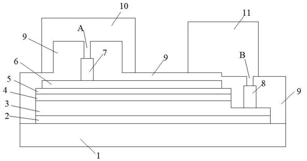
[0035] see figure 1 , a simple eutectic LED chip structure, including a P electrode 7, an N electrode 8, a Bragg reflective layer 9, a P welding layer 10, and an N welding layer 11; the P electrode 7 is arranged below the Bragg reflective layer 9, and Connect to the P welding layer 10 through the first through hole A that penetrates the Bragg reflective layer 9; the N electrode 8 is arranged below the Bragg reflective layer 9, and connects to the N solder layer through the second through hole B that penetrates the Bragg reflective layer 9 11 connections;

[0036] The electrode structures of the P welding layer 10 and the N welding layer 11 are Cr layer, Al layer, (Ti layer / Pt layer) n, Au layer and Sn layer which are sequentially stacked on the Bragg reflection layer 9, wherein, Ti Layer / Pt layer means the Ti layer and the Pt layer which are stacked in sequence, n means the number of repetitions of the stacked Ti layer and the Pt layer, and the value of n is 2.

[0037] The ...


PUM


Abstract

The invention provides a simple eutectic LED chip structure and a manufacturing method thereof. The LED chip structure comprises a P electrode, an N electrode, a Bragg reflection layer, a P welding layer, and an N welding layer, wherein the P electrode is arranged below the Bragg reflection layer and is connected with the P welding layer through a first through hole penetrating through the Bragg reflection layer; the N electrode is arranged below the Bragg reflection layer and is connected with the N welding layer through a second through hole penetrating through the Bragg reflection layer; and the electrode structures of the P welding layer and the N welding layer are respectively a Cr layer, an Al layer, (Ti layer / Pt layer)n, an Au layer and a Sn layer which are sequentially stacked on the Bragg reflection layer, and n represents the number of repetition times of the Ti layer and the Pt layer which are stacked. The manufacturing method comprises the steps of manufacturing a step structure, manufacturing a single wafer, manufacturing a P electrode and an N electrode, manufacturing a Bragg reflection layer, and manufacturing a P welding layer and an N welding layer. According to the invention, the eutectic difficulty is greatly reduced.

Description

technical field [0001] The invention relates to the technical field of LED chip structures, in particular to a simple eutectic LED chip structure and a manufacturing method thereof. Background technique [0002] Compared with front-mounted LED chips, flip-chip LED chips have the advantages of low thermal resistance, high current, no wire bonding, and dense arrangement. In recent years, more and more attention has been paid to flip-chip LED chips. Many units and technology companies have invested in research in this area, and their market size and proportion are increasing year by year. Especially in the aspect of mini chips, the market potential is huge. Since the size of the mini chip is small enough, it is not possible to use solder paste when performing eutectic operation on the packaging side, and usually use screen printing. However, doing mini-level screen printing on the packaging side of the mini chip not only increases the difficulty of eutectic, but also increases...

Claims


Application Information

Patent Timeline
IPC IPC(8): H01L33/10H01L33/38H01L33/40H01L33/00
CPCH01L33/10H01L33/38H01L33/40H01L33/005
Inventor 何鹏
Owner XIANGNENG HUALEI OPTOELECTRONICS
Why Eureka
Try Eureka