Spin filtering magnetic tunnel junction, preparation method and equipment
A magnetic tunnel junction and tunnel junction technology, applied in the field of preparation and spin filtering magnetic tunnel junction, can solve the problems of difficult to achieve industrialization, the tunneling magnetoresistance rate is not high enough, and it is difficult to realize industrialized production, etc., and achieve a huge tunneling magnetoresistance. rate effect
- Summary
- Abstract
- Description
- Claims
- Application Information
AI Technical Summary
Problems solved by technology
Method used
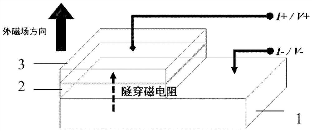
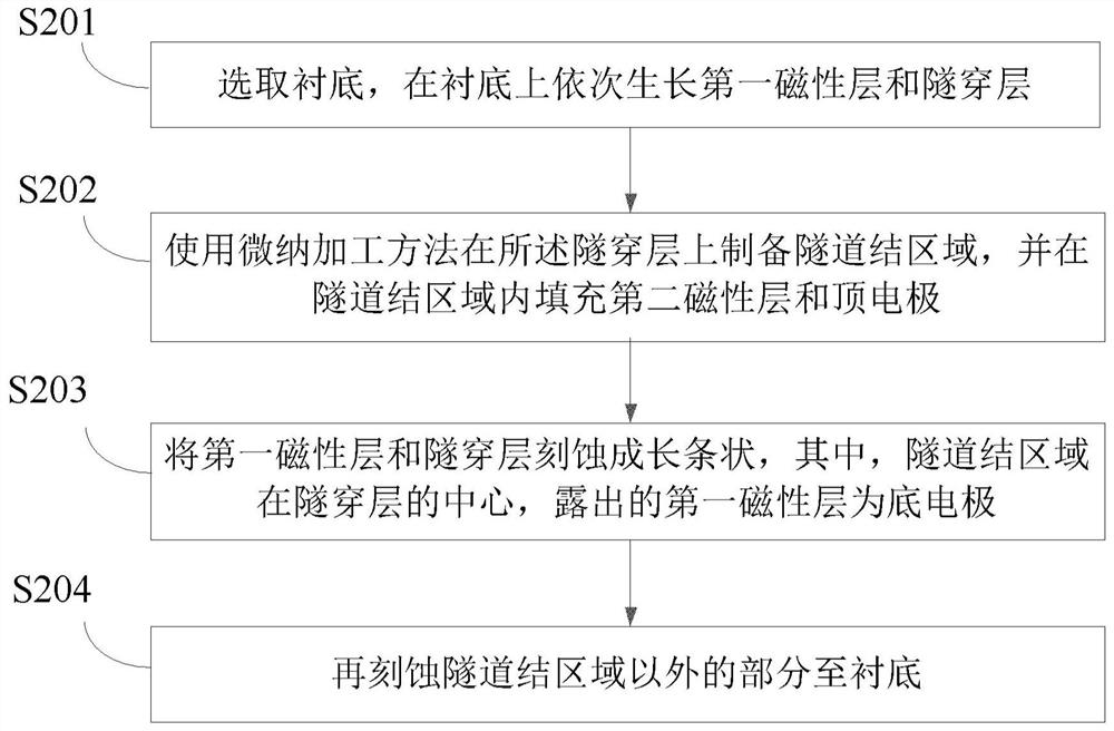
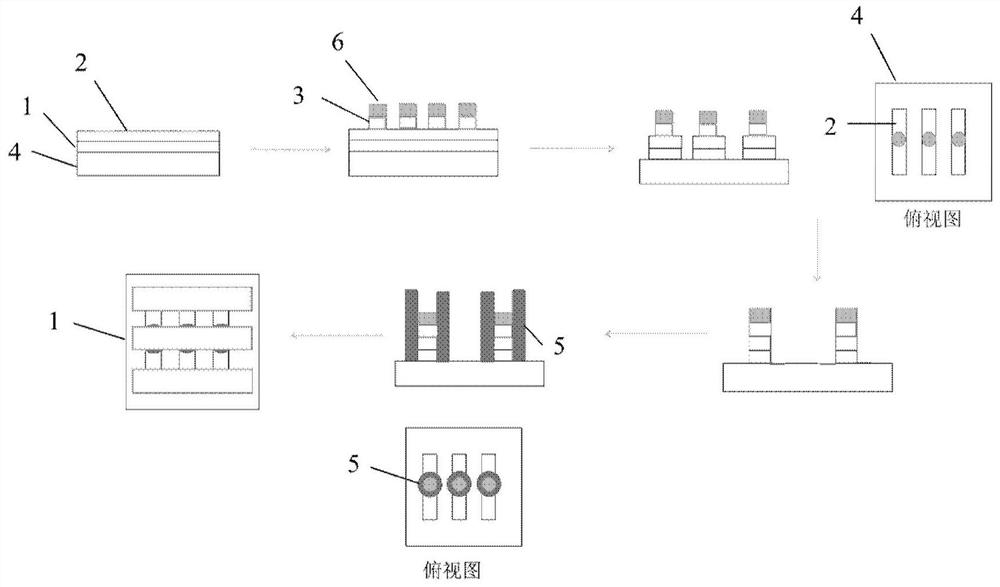
Image

Examples
Embodiment Construction
[0032] Hereinafter, embodiments of the present disclosure will be described with reference to the drawings. It should be understood, however, that these descriptions are exemplary only, and are not intended to limit the scope of the present disclosure. In the following detailed description, for purposes of explanation, numerous specific details are set forth in order to provide a thorough understanding of the embodiments of the present disclosure. It may be evident, however, that one or more embodiments may be practiced without these specific details. Also, in the following description, descriptions of well-known structures and techniques are omitted to avoid unnecessarily obscuring the concept of the present disclosure.
[0033] The terminology used herein is for the purpose of describing particular embodiments only, and is not intended to be limiting of the present disclosure. The terms "comprising", "comprising", etc. used herein indicate the presence of stated features, ...
PUM
| Property | Measurement | Unit |
|---|---|---|
| thickness | aaaaa | aaaaa |
| thickness | aaaaa | aaaaa |
Abstract
Description
Claims
Application Information
 - R&D Engineer
- R&D Manager
- IP Professional
- Industry Leading Data Capabilities
- Powerful AI technology
- Patent DNA Extraction
Browse by: Latest US Patents, China's latest patents, Technical Efficacy Thesaurus, Application Domain, Technology Topic.
© 2024 PatSnap. All rights reserved.Legal|Privacy policy|Modern Slavery Act Transparency Statement|Sitemap