Semiconductor cleaning method and cleaning equipment

A technology for cleaning equipment and semiconductors, which is applied in semiconductor/solid-state device manufacturing, electrical components, circuits, etc. It can solve the problems that affect the performance of semiconductor devices, and semiconductor devices are easy to produce particles, so as to avoid the effect of impact

Pending Publication Date: 2021-12-31
YANGTZE MEMORY TECH CO LTD
View PDF0 Cites 0 Cited by
  • Summary
  • Abstract
  • Description
  • Claims
  • Application Information

AI Technical Summary

Problems solved by technology

However, after cleaning with existing cleaning equipment, the surface of semiconductor devices is prone to produce particles, which will affect the performance of semiconductor devices

Method used


Image

  • Semiconductor cleaning method and cleaning equipment
  • Semiconductor cleaning method and cleaning equipment
  • Semiconductor cleaning method and cleaning equipment

Examples


Embodiment Construction

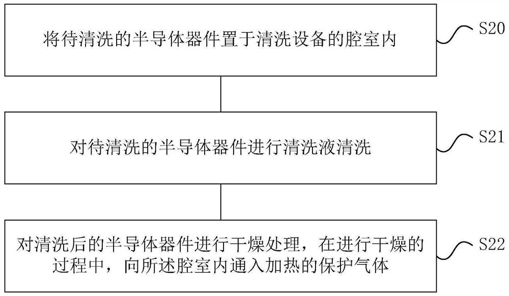
[0026] The specific implementations of the semiconductor cleaning method and cleaning equipment provided by the present invention will be described in detail below in conjunction with the accompanying drawings.

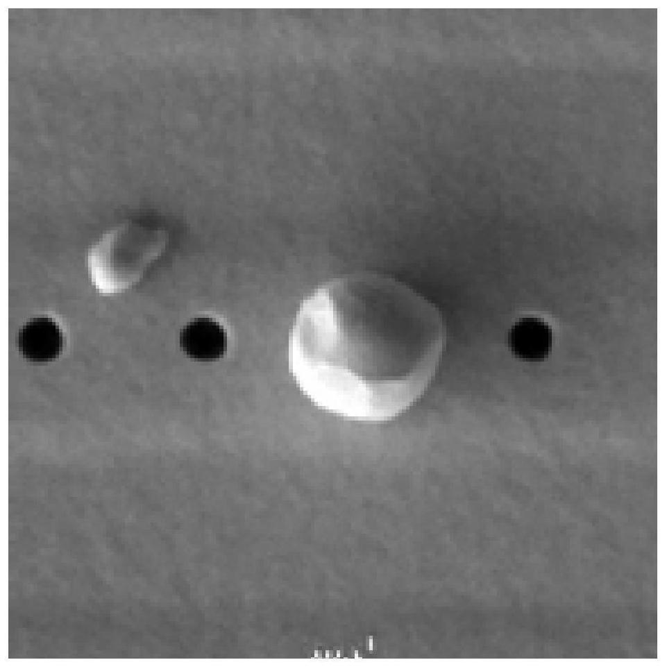
[0027] As mentioned in the background, during the manufacturing process of semiconductor devices, the process of cleaning the semiconductor devices is often involved. The inventors found that after the cleaning process, particles tend to adhere to the surface of the semiconductor device, and the particles will affect the subsequent manufacture of the semiconductor device. figure 1 is the scanning electron microscope image of the surface of the semiconductor device after the cleaning treatment step, from figure 1 It can be seen that particles are attached to the surface of the semiconductor device.

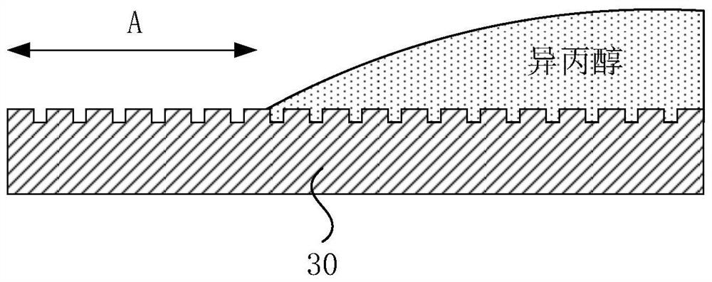
[0028] The inventors further found that the particles exist in the form of solid matter or condensed liquid droplets. The inventor conducted a lot of research and analys...


PUM


Abstract

The invention provides a semiconductor cleaning method and cleaning equipment, and the method is used for cleaning a semiconductor device, and the method comprises the steps: placing the to-be-cleaned semiconductor device in a cavity of the cleaning equipment for cleaning treatment, the cleaning treatment comprising a cleaning fluid cleaning step and a drying step, and at least in the drying step, introducing heated protective gas into the cavity. The embodiment of the invention has the advantages that the heated protective gas can reduce the humidity of the chamber and increase the temperature of the surface of the semiconductor device, so that suspended matters in the chamber are prevented from re-condensing on the surface of the semiconductor device, particulate matters cannot be attached to the surface of the semiconductor device, and the influence on the semiconductor device is avoided.

Description

technical field [0001] The invention relates to the field of integrated circuit manufacturing, in particular to a semiconductor cleaning method and cleaning equipment. Background technique [0002] In the manufacturing process of semiconductor devices, the process of cleaning semiconductor devices is often involved, and even the cleaning process accounts for an increasing proportion. For example, for 3D NAND memory, as the number of word line (WL) layers of 3D NAND memory becomes higher and higher, the line width becomes smaller and smaller. When performing the wet etching process, in order to minimize defects (defect) , the proportion of single chip cleaning is increasing. However, after cleaning with existing cleaning equipment, particles are likely to be generated on the surface of the semiconductor device, which affects the performance of the semiconductor device. Contents of the invention [0003] The technical problem to be solved by the present invention is to pro...

Claims


Application Information

Patent Timeline
Patent Type & Authority Applications(China)
IPC IPC(8): H01L21/67H01L21/02
CPCH01L21/6704H01L21/67034H01L21/67109H01L21/02057
Inventor 宋冬门
Owner YANGTZE MEMORY TECH CO LTD
Why Eureka
Try Eureka