Mode control semiconductor device and preparation method thereof

A mode control and semiconductor technology, applied in the direction of semiconductor lasers, optical waveguide semiconductor structures, lasers, etc., can solve the problem of power coupling loss, increased failure of light-emitting semiconductor devices, and increased power density that cannot be improved at the same time as the anti-optical catastrophe damage threshold of the front cavity surface and other issues, to achieve the effects of cost reduction, reduced coupling loss, and easy preparation

Active Publication Date: 2021-12-31
SUZHOU EVERBRIGHT PHOTONICS CO LTD +1
View PDF10 Cites 0 Cited by
  • Summary
  • Abstract
  • Description
  • Claims
  • Application Information

AI Technical Summary

Problems solved by technology

This increases the power density borne by the cavity surface of the light-emitting semiconductor device, leading to an increase in the failure of the cavity surface optical catastrophe damage of the light-emitting semiconductor device
[0004] At present, the existing technology cannot reduce the coupling loss, production process complexity and cost while improving the anti-optical catastrophe damage threshold power of the front cavity surface

Method used


Image

  • Mode control semiconductor device and preparation method thereof
  • Mode control semiconductor device and preparation method thereof
  • Mode control semiconductor device and preparation method thereof

Examples


Embodiment Construction

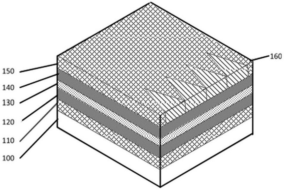
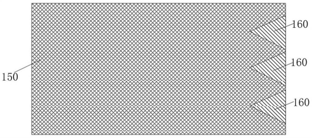
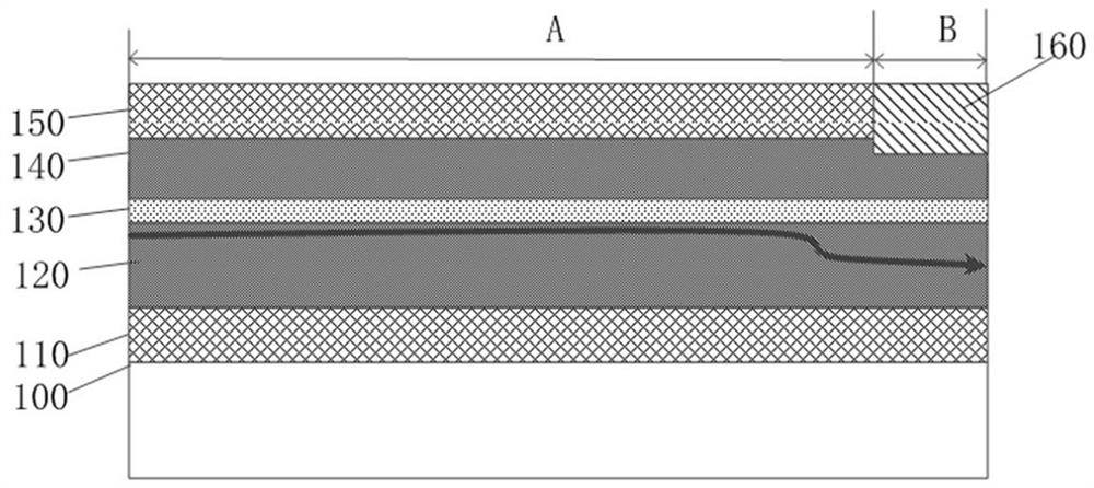
[0032] Light-emitting semiconductor devices are more prone to damage in the active gain region of the cavity surface when the optical power output is high. In order to solve the problem of increased failure of light-emitting semiconductor devices due to optical catastrophe damage on the cavity surface, a method includes: passivating the cavity surface by ultra-high vacuum cleavage, and forming a window structure on the cavity surface in a hybrid way to improve the cavity surface damage resistance. However, these current solutions have extremely strict requirements on the control of process equipment and process conditions, which increases the process complexity and cost of light-emitting semiconductor device production. Another method includes: increasing the power by reducing the optical confinement of the gain material through the design of the epitaxial structure of the chip. However, this method will increase the threshold of the light-emitting semiconductor device and red...


PUM

PropertyMeasurementUnit
thicknessaaaaaaaaaa
thicknessaaaaaaaaaa
thicknessaaaaaaaaaa

Abstract

The invention provides a mode control semiconductor device and a preparation method thereof, the mode control semiconductor device is provided with a front cavity surface and a rear cavity surface which are oppositely arranged, and the mode control semiconductor device comprises a semiconductor substrate layer, an active layer positioned on the semiconductor substrate layer, a first limiting layer and a second limiting layer located on the semiconductor substrate layer and located on the two sides of the active layer respectively, a first waveguide layer located between the first limiting layer and the active layer, a second waveguide layer located between the second limiting layer and the active layer, and having the thickness smaller than or equal to that of the first waveguide layer, and a first dimming layer located in the part, adjacent to the front cavity surface, of the second limiting layer; the refractive index of the first dimming layer is smaller than that of the second limiting layer, and the width of the first dimming layer is gradually increased in the direction from the rear cavity surface to the front cavity surface. According to the mode control semiconductor device, the optical catastrophe damage resistance threshold power of the front cavity surface is improved, and meanwhile, the coupling loss, the production process complexity and the cost are reduced.

Description

technical field [0001] The invention relates to the technical field of semiconductors, in particular to a mode control semiconductor device and a preparation method thereof. Background technique [0002] A light-emitting semiconductor device is a device that produces stimulated emission with a certain semiconductor material as a working substance. Its working principle is: through a certain excitation method, between the energy band (conduction band and valence band) of the semiconductor material, or Between the energy band of the material and the energy level of the impurity (acceptor or donor), the particle number inversion of the non-equilibrium carrier is realized. When a large number of electrons and holes in the particle number inversion state recombine, stimulated emission occurs Because of its small size and high electro-optical conversion efficiency, light-emitting semiconductor devices are widely used. [0003] The development direction of high-power light-emittin...

Claims


Application Information

Patent Timeline
Patent Type & Authority Applications(China)
IPC IPC(8): H01S5/20
CPCH01S5/2018H01S5/2031
Inventor 谭少阳王俊刘停停李泉灵廖新胜闵大勇
Owner SUZHOU EVERBRIGHT PHOTONICS CO LTD
Why Eureka
Try Eureka