PCB manufacturing method and PCB

A technology for PCB boards and manufacturing methods, applied in multilayer circuit manufacturing, printed circuit manufacturing, electrical components, etc., can solve problems such as easy pollution of the environment, low production efficiency, and increased production costs, so as to avoid environmental pollution and improve production efficiency Effect

Pending Publication Date: 2022-01-11
ELEC & ELTEK GUANGZHOU ELECTRONICS
View PDF0 Cites 0 Cited by
  • Summary
  • Abstract
  • Description
  • Claims
  • Application Information

AI Technical Summary

Problems solved by technology

[0003] At present, in the production process of PCB board, before immersion gold treatment, it is necessary to use adhesive tape to cover the edge of the waste area of ​​PCB board, so as to reduce the consumption of gold salt in immersion gold treatment, thereby saving costs; after immersion gold treatment, also The tape needs to be removed manually, which leads to low production efficiency, and it is difficult to handle the tape, which is easy to pollute the environment; and the use of tape wrapping has the following disadvantages: it needs to purchase an additional rubber wrapping machine with a higher price, which increases production costs, and the edge of the tape remains heavy gold After using the liquid medicine, it will affect the production quality of the PCB board, and the residual liquid medicine is easy to cause environmental pollution; therefore, there is an urgent need for a PCB board manufacturing method without adhesive tape coating

Method used


Image

  • PCB manufacturing method and PCB
  • PCB manufacturing method and PCB
  • PCB manufacturing method and PCB

Examples


Embodiment Construction

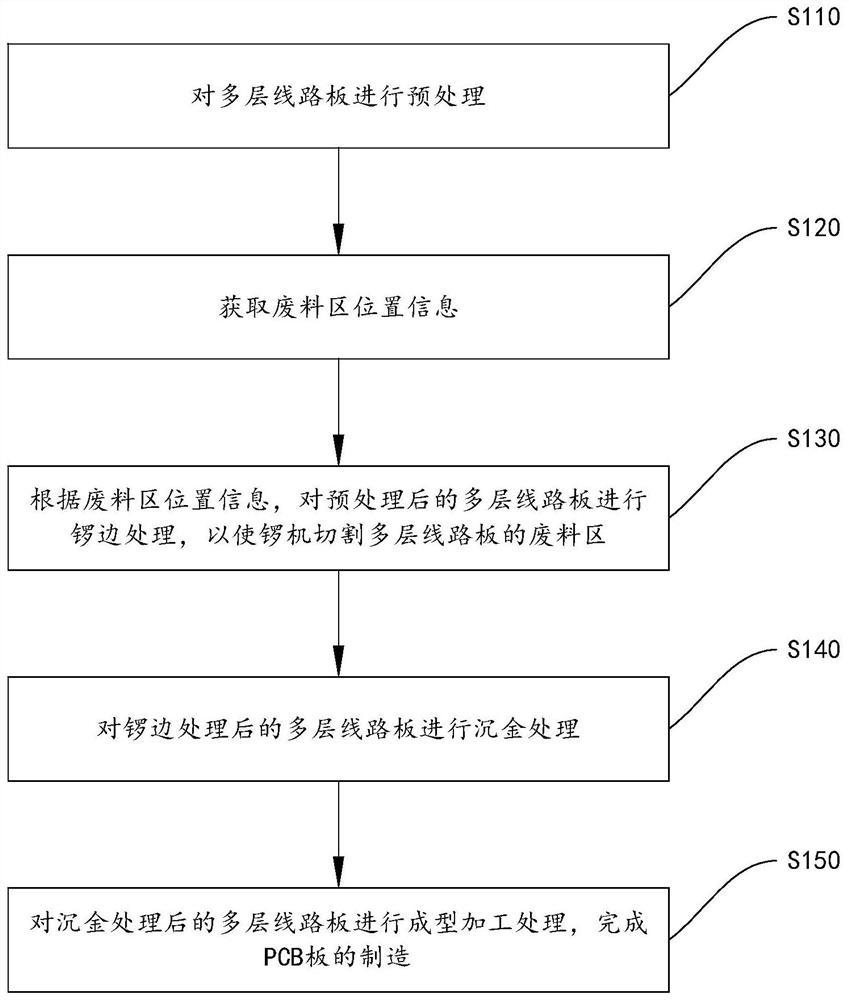
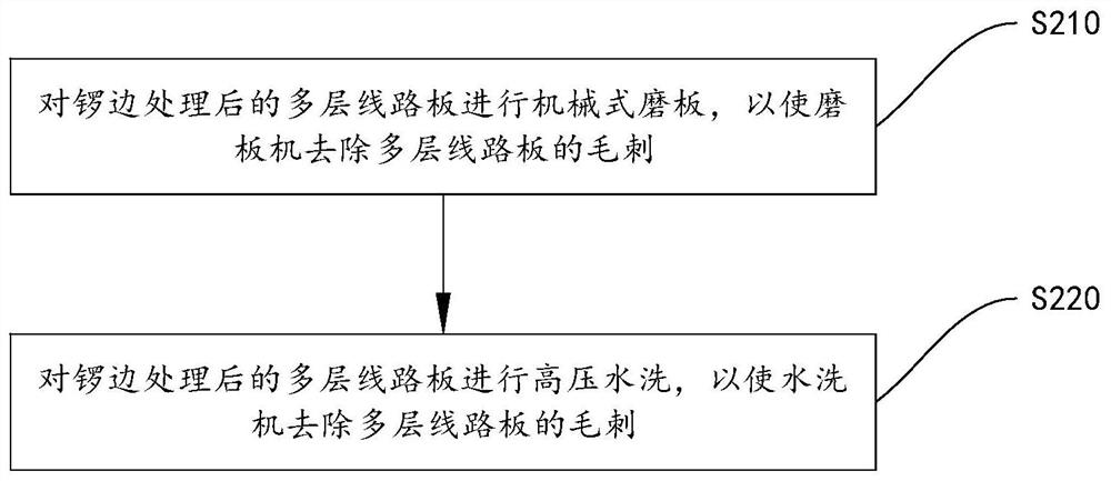
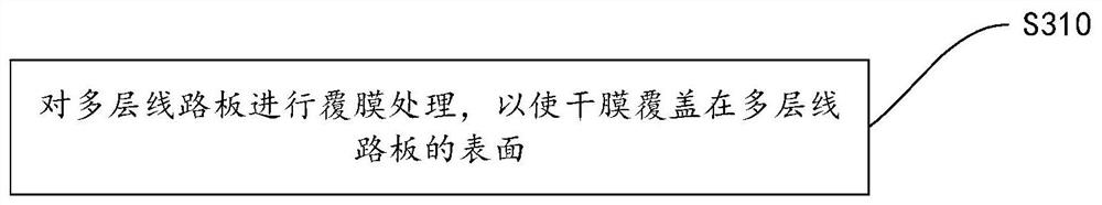
[0026] In order to make the objectives, technical solutions and advantages of the present invention clearer, the present invention will be further described in detail below with reference to the accompanying drawings and embodiments. It should be understood that the specific embodiments described herein are only used to explain the present invention, but not to limit the present invention.

[0027] It should be noted that although the functional modules are divided in the schematic diagram of the device, and the logical sequence is shown in the flowchart, in some cases, the modules may be divided differently from the device, or executed in the order in the flowchart. steps shown or described. The terms "first", "second" and the like in the description and claims and the above drawings are used to distinguish similar objects and are not necessarily used to describe a specific order or sequence.

[0028] Unless otherwise defined, all technical and scientific terms used herein h...


PUM


Abstract

The invention discloses a PCB (Printed Circuit Board) manufacturing method and a PCB. The method comprises the following steps of: pre-processing a multi-layer circuit board; acquiring waste material area position information; according to the waste material area position information, carrying out edge milling treatment on the preprocessed multilayer circuit board so that a milling machine can cut the waste material area of the multi-layer circuit board; performing gold immersion treatment on the multilayer circuit board after the edge milling treatment; and carrying out forming processing on the multilayer circuit board after gold immersion treatment to complete manufacturing of the PCB. According to the scheme provided by the embodiment of the invention, the position information of the waste area can be obtained, and the waste area of the multilayer circuit board is cut through the milling machine, so that the multilayer circuit board without the edge of the waste area is subjected to gold immersion treatment, the PCB manufacturing method without adhesive tape coating is realized, the production efficiency is effectively improved, and the environment pollution is avoided.

Description

technical field [0001] The invention relates to the technical field of PCB boards, in particular to a method for manufacturing a PCB board and a PCB board. Background technique [0002] The printed circuit board, that is, the PCB board, is on one, several, or dozens of insulating boards, using the printing method, coating the wires, etching the micropores, and then laminating them layer by layer to achieve Electrical interconnection between layers. Then, various chips, resistors, capacitors, inductors and other devices are installed on the PCB board, and after a certain amount of packaging, an electronic product capable of specific computing functions is completed. As mentioned above, the role of the PCB board is twofold: one is the mechanical aspect, which is to provide mechanical support for the devices on it; the other is the electrical aspect, which is to provide circuit conduction and isolation for the devices on it. [0003] At present, in the production process of P...

Claims


Application Information

Patent Timeline
Patent Type & Authority Applications(China)
IPC IPC(8): H05K3/46
CPCH05K3/4611
Inventor 张伟连
Owner ELEC & ELTEK GUANGZHOU ELECTRONICS
Why Eureka
Try Eureka