
PCB automatic forming and milling system

An automatic forming and PCB board technology, which is applied in the direction of milling machine equipment, milling machine equipment details, electrical components, etc., can solve the problems of cumbersome production method steps, difficult operation, danger, etc., and achieve the goal of simplifying the fixed structure of PCB board and improving production efficiency Effect

Pending Publication Date: 2022-01-21
深圳市众博信发展有限公司
View PDF0 Cites 0 Cited by
  • Summary
  • Abstract
  • Description
  • Claims
  • Application Information

AI Technical Summary

Problems solved by technology

[0003] But above-mentioned production method step is extremely loaded down with trivial details, at first, needs to all process positioning hole 3 at the four corner positions of each finished circuit board 2, and its positioning method is very complicated and inefficient; In the process of separating the finished circuit boards 2 one by one, since the way of separating one by one will destroy the overall structural characteristics of the entire raw material board 1, it is necessary to manually track and take them at any time during the separation process. The separated finished circuit board 2 is difficult to operate and has a certain degree of danger, which is the main shortcoming of the traditional technology

Method used


Image

  • PCB automatic forming and milling system
  • PCB automatic forming and milling system
  • PCB automatic forming and milling system

Examples


Embodiment Construction

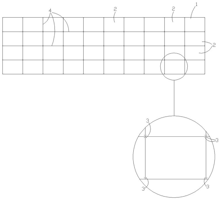
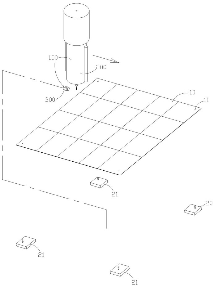
[0019] Such as Figures 1 to 10 As shown, a PCB board automatic forming milling system 100 includes a cutting milling cutter 200 and a powder solidification unit 300 .

[0020] The cutting milling cutter 200 includes a rotating shaft 210 , a cutter head 220 and a powder involuting cavity 230 , wherein the cutter head 220 is fixedly disposed below the rotating shaft 210 .

[0021] When the cutter head 220 rotates, the powder involute cavity 230 is formed under the rotating shaft 210 .

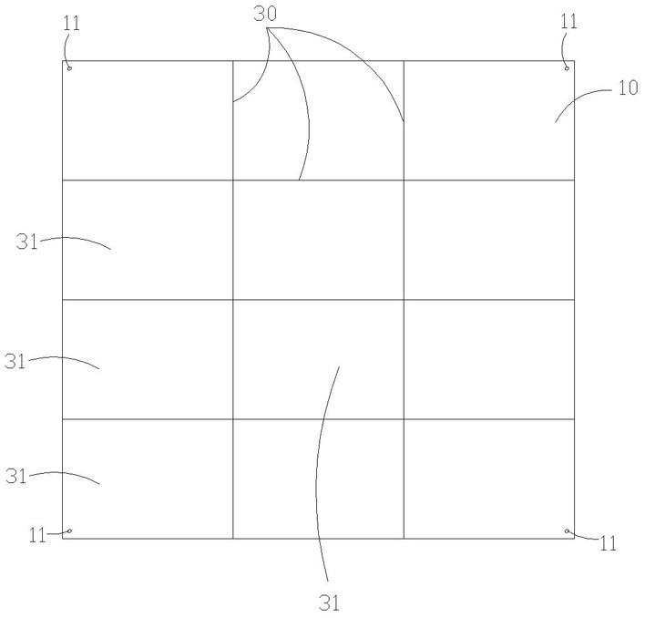
[0022] When working, at first, the positioning holes 11 are processed at the four corners of the PCB raw material board 10, and the PCB raw material board 10 is fixed on the milling machine processing table. The four corners of the milling machine table are provided with positioning pins 20 . The positioning pin 20 is correspondingly set in the positioning hole 11 of the PCB material board 10 to fix and position the PCB material board 10 . During specific implementation, a square backing plat...


PUM


Abstract

The invention relates to a PCB automatic forming and milling system. The system comprises a cutting milling cutter and a powder curing unit; the cutting milling cutter comprises a rotating shaft, a cutter head and a powder inner rolling cavity; during working, PCB raw material boards are fixed on a milling machine machining table, multiple calibration lines are generated on the PCB raw material boards, the cutting milling cutter carries out milling action along the calibration lines, and easy-to-break grooves are formed in the positions of the calibration lines; and the powder curing unit is arranged below the cutting milling cutter, the powder curing unit comprises an extrusion curing device and a cooling curing device, the extrusion curing device is used for generating upward jacking extrusion acting force, and the cooling curing device is used for cooling the extrusion curing device.

Description

technical field [0001] The invention relates to a forming and milling system, in particular to a system for batch forming and milling an entire PCB raw material board. Background technique [0002] Such as figure 1 As shown, at present, the mass production of PCB boards is generally carried out in the following manner. The first step is to produce the entire raw material board 1, the second step is to process the circuit layer on the entire raw material board 1, and the second step is to process the circuit layer on the entire raw material board 1. The third step is to generate several finished circuit boards 2 on the entire raw material board 1, the fourth step is to process positioning holes 3 at the four corners of each finished circuit board 2, and the fifth step is to place the entire raw material board 1 is fixed on the milling machine, and each finished circuit board 2 is positioned through the positioning hole 3. In the sixth step, the milling cutter is used to cut ...

Claims


Application Information

Patent Timeline
Patent Type & Authority Applications(China)
IPC IPC(8): B23C3/00H05K3/00
CPCB23C3/00H05K3/0044
Inventor 袁卫成
Owner 深圳市众博信发展有限公司
Learn More