Check patentability & draft patents in minutes with Patsnap Eureka AI!

Photomask defect detection method and system

A defect detection and detection system technology, applied in the directions of optical testing flaws/defects, optics, measuring devices, etc., can solve the problems of increased production costs, wafer rework, etc., and achieve the effect of reducing the rework rate and production cost

Active Publication Date: 2022-01-25
CHANGXIN MEMORY TECH INC
View PDF6 Cites 0 Cited by
  • Summary
  • Abstract
  • Description
  • Claims
  • Application Information

AI Technical Summary

Problems solved by technology

[0003]Because the mask is used continuously before cleaning is detected, particles or other defects on the surface of the mask (reticle defects mainly include haze defects , particle dust, scratches, etc.) will continue to affect the process during use. If there are dust particles or other defects that exceed the specification on the mask, all the wafers that have been subjected to the photolithography process will be reworked , resulting in increased production costs

Method used


Image

  • Photomask defect detection method and system
  • Photomask defect detection method and system
  • Photomask defect detection method and system

Examples


Embodiment Construction

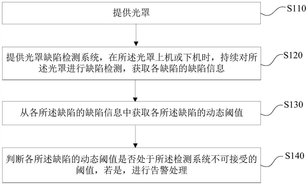
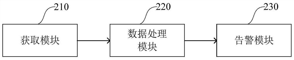
[0034] In order to facilitate the understanding of the present invention, the present invention will be described more fully below with reference to the associated drawings. Embodiments of the invention are shown in the drawings. However, the present invention can be embodied in many different forms and is not limited to the embodiments described herein. Rather, these embodiments are provided so that the disclosure of the present invention will be thorough and complete.

[0035] Unless otherwise defined, all technical and scientific terms used herein have the same meaning as commonly understood by one of ordinary skill in the technical field of the invention. The terms used herein in the description of the present invention are for the purpose of describing specific embodiments only, and are not intended to limit the present invention.

[0036] When used herein, the singular forms "a", "an" and "the / the" may also include the plural forms unless the context clearly dictates o...


PUM


Abstract

The invention relates to a photomask defect detection method and system. The photomask defect detection method comprises the following steps: providing a photomask; providing a photomask defect detection system, continuously performing defect detection on the photomask when the photomask is loaded or unloaded, and obtaining defect information of each defect; obtaining a dynamic threshold value of each defect from the defect information of each defect; and judging whether the dynamic threshold value of each defect belongs to a threshold value unacceptable by the detection system, and if so, carrying out alarm processing.

Description

technical field [0001] The invention relates to the technical field of integrated circuits, in particular to a method and system for detecting defects in a photomask. Background technique [0002] In the manufacturing process of semiconductor devices such as dynamic random access memory (Dynamic Random Access Memory, DRAM), photolithography is a crucial step. In the photolithography process, the photomask plays a very important role. The quality of the photomask directly affects the yield rate of semiconductor products, so the quality of the photomask has become a necessary process. [0003] Since the mask is continuously used before it is detected that it needs to be cleaned, particles or other defects on the surface of the mask (reticle defects mainly include foggy defects, particle dust, scratches, etc.) will continue to affect the surface of the mask during use. The process is affected. If there are dust particles or other defects that exceed the specification on the ma...

Claims


Application Information

Patent Timeline
IPC IPC(8): G01N21/94G01N21/958
CPCG01N21/94G01N21/958G01N2021/945G03F1/84
Inventor 侯力华许文豪
Owner CHANGXIN MEMORY TECH INC
Features
  • R&D
  • Intellectual Property
  • Life Sciences
  • Materials
  • Tech Scout
  • Unparalleled Data Quality
  • Higher Quality Content
  • 60% Fewer Hallucinations
Learn More