Silicon wafer slicing device for bipolar transistor production

A bipolar transistor and slicing device technology, which is applied in semiconductor/solid-state device manufacturing, electrical components, circuits, etc., can solve the problems of uneven slicing of silicon wafers, labor-saving slicing, etc.

Active Publication Date: 2018-01-23
谱罗顿智控电子科技(浙江)有限公司
View PDF10 Cites 11 Cited by
  • Summary
  • Abstract
  • Description
  • Claims
  • Application Information

AI Technical Summary

Problems solved by technology

[0006] In order to overcome the shortcomings of uneven and labor-saving slicing of silicon wafers in the prior art, the technical problem to be solved by the present invention is to provide a silicon wafer for bipolar transistor production that can be sliced ​​evenly and can save labor. slicer

Method used


Image

  • Silicon wafer slicing device for bipolar transistor production
  • Silicon wafer slicing device for bipolar transistor production
  • Silicon wafer slicing device for bipolar transistor production

Examples


Embodiment 1

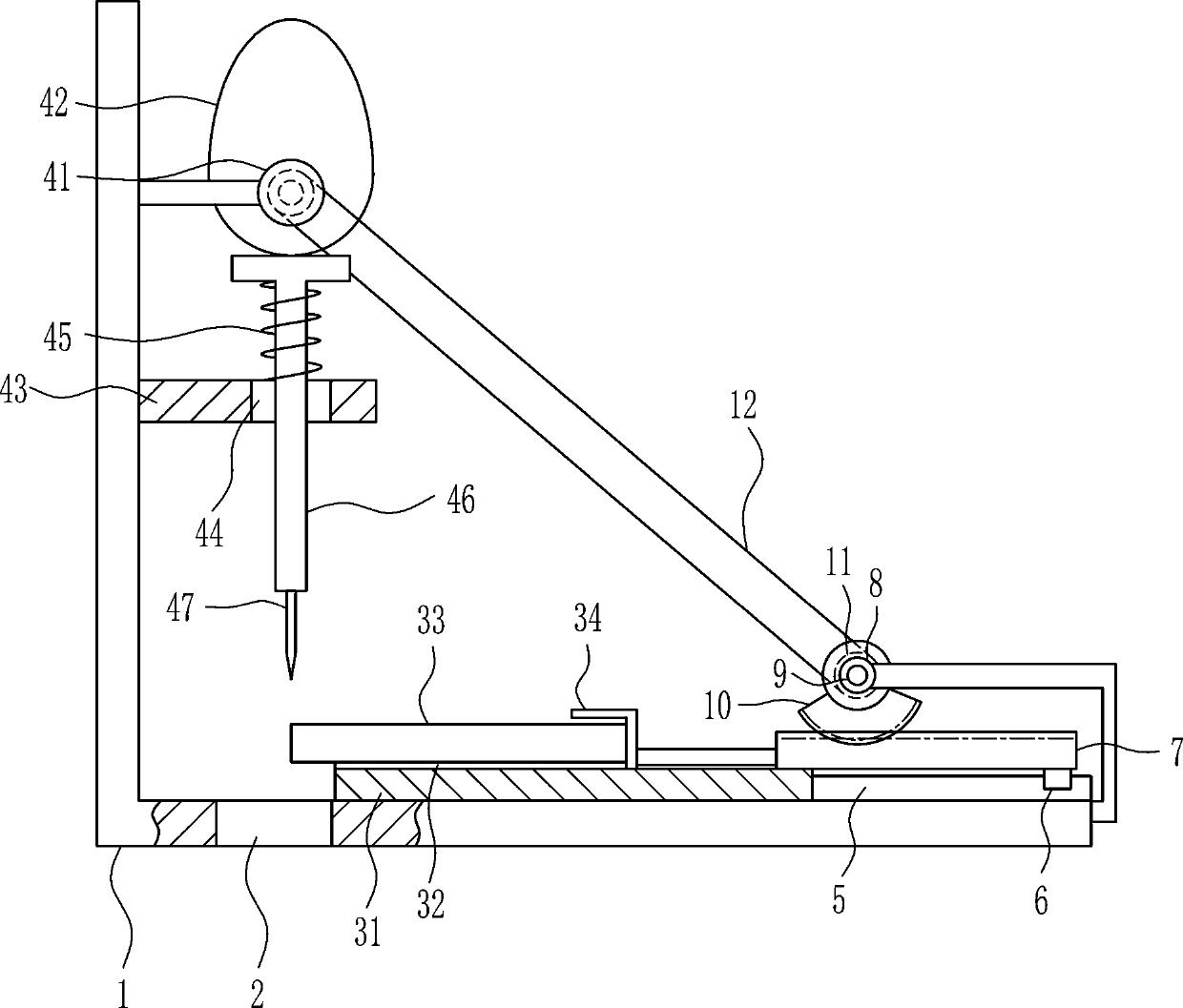
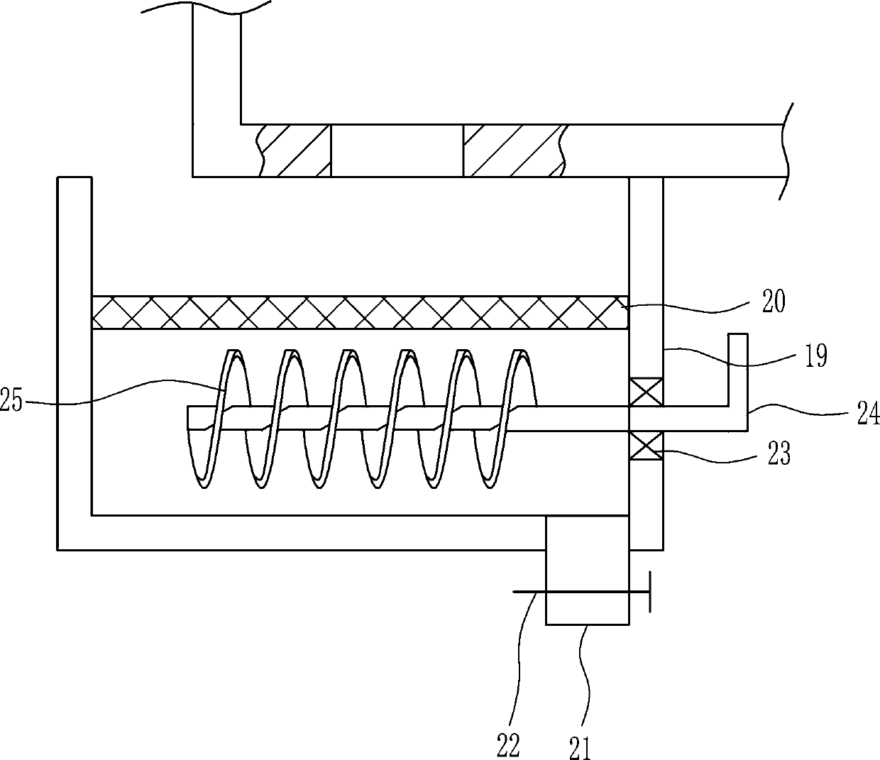
[0034] A device for slicing silicon wafers for the production of bipolar transistors, such as Figure 1-7 As shown, it includes a mounting frame 1, a cutting mechanism 4 and a pushing mechanism 3. The bottom left side of the mounting frame 1 has a through hole 2, the upper part of the mounting frame 1 is provided with a cutting mechanism 4, and the lower part of the mounting frame 1 is provided with a pushing mechanism. 3. The pushing mechanism 3 and the cutting mechanism 4 cooperate with each other.

Embodiment 2

[0036] A device for slicing silicon wafers for the production of bipolar transistors, such as Figure 1-7 As shown, it includes a mounting frame 1, a cutting mechanism 4 and a pushing mechanism 3. The bottom left side of the mounting frame 1 has a through hole 2, the upper part of the mounting frame 1 is provided with a cutting mechanism 4, and the lower part of the mounting frame 1 is provided with a pushing mechanism. 3. The pushing mechanism 3 and the cutting mechanism 4 cooperate with each other.

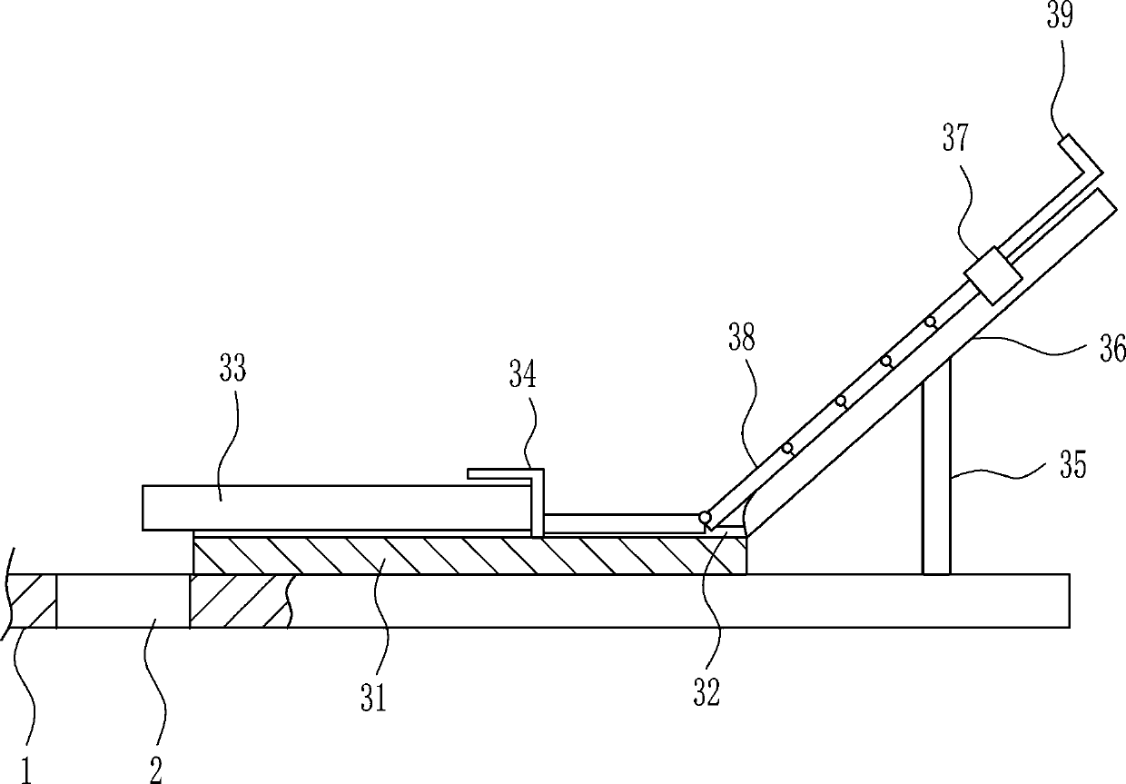
[0037] The pushing mechanism 3 includes a mounting rod 31, a silicon body 33, a push rod 34, a support rod 35, a first slide rail 36, a first slider 37, a first connecting rod 38 and a handle 39, and the top of the mounting frame 1 is connected with a mounting Rod 31, the top of the mounting rod 31 is provided with a placement groove 32, a silicon body 33 is placed on the left side of the placement groove 32, a push rod 34 is placed on the right side of the placement groove 32, ...

Embodiment 3

[0039] A device for slicing silicon wafers for the production of bipolar transistors, such as Figure 1-7 As shown, it includes a mounting frame 1, a cutting mechanism 4 and a pushing mechanism 3. The bottom left side of the mounting frame 1 has a through hole 2, the upper part of the mounting frame 1 is provided with a cutting mechanism 4, and the lower part of the mounting frame 1 is provided with a pushing mechanism. 3. The pushing mechanism 3 and the cutting mechanism 4 cooperate with each other.

[0040] The pushing mechanism 3 includes a mounting rod 31, a silicon body 33, a push rod 34, a support rod 35, a first slide rail 36, a first slider 37, a first connecting rod 38 and a handle 39, and the top of the mounting frame 1 is connected with a mounting Rod 31, the top of the mounting rod 31 is provided with a placement groove 32, a silicon body 33 is placed on the left side of the placement groove 32, a push rod 34 is placed on the right side of the placement groove 32, ...


PUM


Abstract

The invention relates to a slicing device, in particular to a silicon wafer slicing device for bipolar transistor production. The invention provides the silicon wafer slicing device, which can be usedfor uniformly cutting a silicon wafer and can be labor-saving, for the bipolar transistor production. In order to solve the technical problem, the silicon wafer slicing device for the bipolar transistor production, provided by the invention, comprises an installation rack, wherein a through hole is formed in a left side of the bottom part of the installation rack, a cutting mechanism is arrangedat an upper part of the installation rack, a push mechanism is arranged at a lower part of the installation rack, and the push mechanism is matched with the cutting mechanism. The silicon wafer slicing device for the bipolar transistor production is arranged, the push mechanism and the cutting mechanism are arranged, a silicon body can be constantly cut and sliced by a cutter, so that the operation of silicon body slicing is completed; and a belt pulley and a flat belt are arranged, the silicon body is not needed to be pushed by manual, so that the silicon wafer cutting is more accurate and uniform, and the working efficiency is further improved.

Description

technical field [0001] The invention relates to a slicing device, in particular to a silicon chip slicing device for bipolar transistor production. Background technique [0002] A transistor composed of two back-to-back PN structures to obtain voltage, current or signal gain. It originated from the point-contact transistor transistor invented in 1948, and developed into a junction transistor in the early 1950s, which is now called a bipolar transistor. There are two basic structures of bipolar transistors: PNP type and NPN type. In these three layers of semiconductors, the middle layer is called the base region, and the outer two layers are called the emitter region and the collector region. When a small amount of current is injected into the base region, a larger current will form between the emitter region and the collector region, which is the amplification effect of the transistor. [0003] The production of bipolar transistors requires silicon wafers. The silicon waf...

Claims


Application Information

Patent Timeline
Patent Type & Authority Applications(China)
IPC IPC(8): H01L21/304H01L21/331
Inventor 陈政
Owner 谱罗顿智控电子科技(浙江)有限公司
Why Eureka
Try Eureka