Touch display panel and display device

A touch display panel and touch display technology, which is applied in the directions of instruments, computing, and electrical digital data processing, etc., can solve problems such as increased bonding pads, large yield loss, and enlarged bonding pin area. Achieve the effects of reducing the number of bonding processes, realizing narrower edges, and improving yield

Active Publication Date: 2022-02-25
CHANGSHA HKC OPTOELECTRONICS CO LTD +1
View PDF8 Cites 0 Cited by
  • Summary
  • Abstract
  • Description
  • Claims
  • Application Information

AI Technical Summary

Problems solved by technology

[0003] However, the conventional InCell touch display panel structure requires additional touch pads on the display panel to transmit touch signals, resulting in more bonding pads and larger bonding pin areas, which is not conducive to narrow bezel products. At the same time, because the touch pad and the pad used to transmit the display signal need to perform two bonding processes, the more the process is, the greater the yield loss

Method used


Image

  • Touch display panel and display device
  • Touch display panel and display device
  • Touch display panel and display device

Examples


Embodiment 1

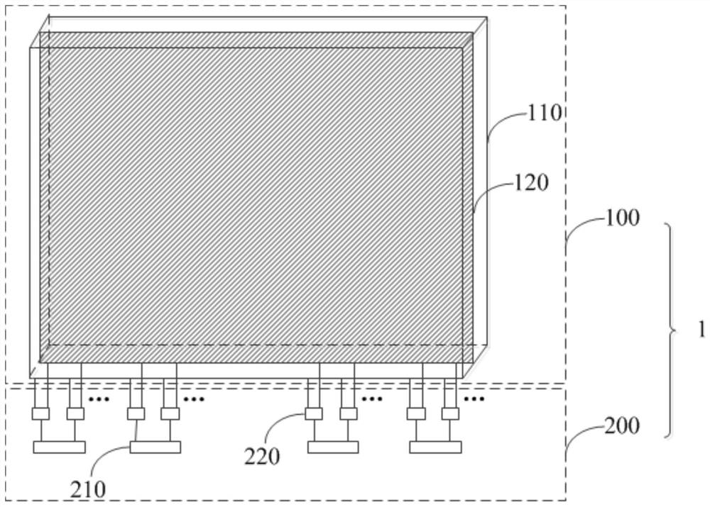
[0042] The first aspect of the embodiments of the present application provides a touch display panel 1 .

[0043] Such as figure 1 As shown, the touch display panel 1 includes:

[0044] The touch display area 100, the touch display area is provided with a display module 110 and a touch module 120 arranged in the display module 110;

[0045] Non-display area 200, non-display area 200 is provided with a plurality of pads 210 and a plurality of time-sharing output circuits 220 for bonding connection chip-on-chip 240, the first end of each time-division output circuit 220 is connected to the corresponding pad 210 are electrically connected, the second end of each time-sharing output circuit 220 is connected to the corresponding signal end of the display module 110, and the third end of each time-sharing output circuit 220 is connected to the corresponding signal end of the touch module 120;

[0046] The pad 210 is used for transmitting display signals, touch signals, display sca...

Embodiment 2

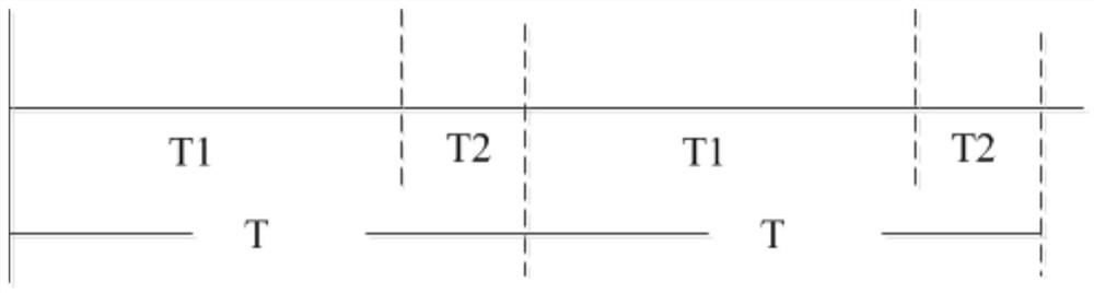
[0069] Such as Figure 4 As shown, optionally, the time-division output circuit 220 includes a first switch circuit 221 and a second switch circuit 222;

[0070] The first end of the first switch circuit 221 is used to connect the pad 210, the second end of the first switch circuit 221 is connected to the first end of the second switch circuit 222 and is used to connect the display signal end of the display module 110, and the second The second end of the switch circuit 222 is used to connect the touch signal end of the touch module 120;

[0071] The controlled end of the first switch circuit 221 is used to input the display scan signal, and is kept normally on;

[0072] The controlled terminal of the second switch circuit 222 is used for inputting the touch scanning signal, and is turned off during the display time T1 in one frame, and turned on during the touch time T2 in one frame.

[0073] In this embodiment, several pads 210 among the multiple pads 210 are used to conne...

Embodiment 3

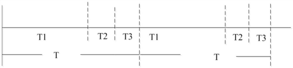
[0078] Such as Image 6 As shown, optionally, the time-division output circuit 220 includes a first switch circuit 221 and a second switch circuit 222;

[0079] The first terminal of the first switch circuit 221 is used to connect the touch signal terminal of the touch module 120 , the second terminal of the first switch circuit 221 is connected to the first terminal of the second switch circuit 222 and used to connect the pad 210 , The second end of the second switch circuit 222 is used to connect to the display signal end of the display module 110;

[0080] The controlled terminal of the first switch circuit 221 is used for inputting the touch scanning signal and is turned off during the display time T1 in one frame, and turned on during the touch time T2 in one frame;

[0081] The controlled end of the second switch circuit 222 is used to input the display scanning signal and is turned on during the display time T1 in one frame, and turned off during the touch time T2 in o...


PUM


Abstract

The invention provides a touch display panel and a display device, and belongs to the field of display panels. The touch display panel comprises a touch display area and a non-display area, the touch display area comprises a display module and a touch control module arranged in the display module. The non-display area is provided with a plurality of gaskets and a plurality of time-sharing output circuits, the gaskets and the time-sharing output circuits are used for being connected with the chip on films in a bonding mode, the time-sharing output circuits are connected with the gaskets used for transmitting display signals and touch signals, and the time-sharing output circuits are communicated with the display module and the gaskets and transmit the display signals within the display time. Therefore, the display module is driven to lighten and display. In the touch control time, the time-sharing output circuit is communicated with the touch module and the gaskets and transmits the touch signal, so that the touch work of the panel is realized, the bonding process frequency is reduced by reusing the gaskets, the yield of the touch display panel is improved, and meanwhile, the edge narrowing of the touch display panel is realized.

Description

technical field [0001] The present application belongs to the technical field of display panels, and in particular relates to a touch display panel and a display device. Background technique [0002] With the rapid development of display technology, touch display panels have been widely accepted and used by people, for example, smart phones, tablet computers, etc. all use touch display panels. The touch display panel adopts the embedded touch technology to integrate the touch panel and the display panel, and embeds the function of the touch panel into the display panel, so that the display panel has the functions of displaying and sensing touch input at the same time. According to different structures, the touch display panel can be divided into a type in which the touch electrodes cover the liquid crystal cell (OnCell), a type in which the touch electrodes are embedded in the liquid crystal cell (InCell), and an external type. Among them, the InCell type has the advantages...

Claims


Application Information

Patent Timeline
Patent Type & Authority Applications(China)
IPC IPC(8): G06F3/041
CPCG06F3/04166G06F3/04164G06F3/0412
Inventor 李旺李荣荣
Owner CHANGSHA HKC OPTOELECTRONICS CO LTD
Why Eureka
Try Eureka