Cross-clock domain data signal synchronization method, system and device and medium

A data signal, cross-clock domain technology, applied in the field of data synchronization, can solve the problems of complex cross-clock processing, asynchronous FIFO increase, and difficult timing convergence, etc., to achieve the effect of reducing the system bus area and improving the system bus efficiency

Pending Publication Date: 2022-03-01
山东云海国创云计算装备产业创新中心有限公司
View PDF0 Cites 2 Cited by
  • Summary
  • Abstract
  • Description
  • Claims
  • Application Information

AI Technical Summary

Problems solved by technology

As the scale of the SOC chip continues to increase, the data bit width between the interfaces is also increasing, and the working clock domains of the interface modules are also different, which makes the cross-clock processing in the bus become complicated and the timing is difficult to converge. In this way, the cross-clock processing logic in the system bus The design of the code presents challenges
[0003] Aiming at the cross-clock domain processing of multi-bit

Method used


Image

  • Cross-clock domain data signal synchronization method, system and device and medium
  • Cross-clock domain data signal synchronization method, system and device and medium
  • Cross-clock domain data signal synchronization method, system and device and medium

Examples


Embodiment Construction

[0042] In order to make the object, technical solution and advantages of the present invention clearer, the embodiments of the present invention will be further described in detail below in conjunction with specific embodiments and with reference to the accompanying drawings.

[0043] It should be noted that all expressions using "first" and "second" in the embodiments of the present invention are to distinguish two entities with the same name but different parameters or parameters that are not the same, see "first" and "second" It is only for the convenience of expression, and should not be construed as a limitation on the embodiments of the present invention, which will not be described one by one in the subsequent embodiments.

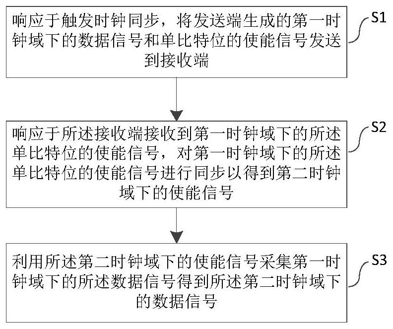
[0044] According to one aspect of the present invention, an embodiment of the present invention proposes a data signal synchronization method across clock domains, such as figure 1 As shown, it may include the steps of:

[0045] S1, in response to ...


PUM


Abstract

The invention discloses a cross-clock domain data signal synchronization method, which comprises the following steps of: in response to triggering clock synchronization, sending a data signal in a first clock domain generated by a sending end and a single-bit enable signal to a receiving end; in response to the single-bit enable signal in a first clock domain received by the receiving end, synchronizing the single-bit enable signal in the first clock domain to obtain an enable signal in a second clock domain; and acquiring the data signal in the first clock domain by using the enable signal in the second clock domain to obtain the data signal in the second clock domain. The invention further discloses a system, computer equipment and a readable storage medium. The scheme provided by the invention can be used for realizing cross-clock domain synchronization of multi-bit wide data signals in the bus.

Description

technical field [0001] The invention relates to the field of data synchronization, in particular to a data signal synchronization method, system, device and storage medium across clock domains. Background technique [0002] The system bus is an important part of the SOC chip, which is used to connect the functional modules in the chip, complete the data transmission between the modules, and ensure that the functional modules are interconnected and run together. As the scale of the SOC chip continues to increase, the data bit width between the interfaces is also increasing, and the working clock domains of the interface modules are also different, which makes the cross-clock processing in the bus become complicated and the timing is difficult to converge. In this way, the cross-clock processing logic in the system bus The design of the code presented challenges. [0003] Aiming at the cross-clock domain processing of multi-bit wide data signals in the system bus, in the exis...

Claims


Application Information

Patent Timeline
IPC IPC(8): G06F1/12
CPCG06F1/12
Inventor 石广刘刚
Owner 山东云海国创云计算装备产业创新中心有限公司
Why Eureka
Try Eureka