Nano metal via hole interconnection method based on thermal shrinkage
A technology of nano metal and nano metal particles, applied in the fields of nanotechnology, nanotechnology, nanotechnology for material and surface science, can solve problems such as processing defects, low hole filling efficiency, failure, etc., to improve electrical and thermal conductivity performance, reduction of machining defects, the effect of a simple method
- Summary
- Abstract
- Description
- Claims
- Application Information
AI Technical Summary
Problems solved by technology
Method used
Image

Examples
Embodiment 1
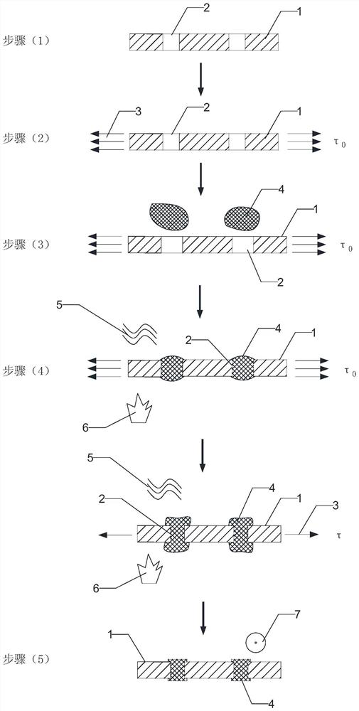
[0034] see figure 1 , this embodiment discloses a thermal shrinkage-based nano-metal via interconnection method, including the following steps:
[0035] (1) Select a material with thermal shrinkage properties or a material with a negative coefficient of thermal expansion as the material of the substrate 1. There is a through hole 2 on the substrate 1, and the diameter of the through hole 2 is D 0 , the depth is h;
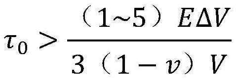
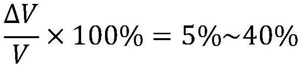
[0036] (2) Using the tensioning device 3, symmetrical tensile stress is applied to both sides of the substrate 1, and the tensile stress initially applied is the initial tensile stress τ 0 , the substrate 1 is subjected to initial tensile stress, so that the substrate 1 is in a state of tensile stress, and the through hole 2 on the substrate 1 expands outward, and the diameter of the through hole 2 is D at this time;
[0037] (3) Select a kind of nano-metal particle 4 as the filling material, and fill the nano-metal particle 4 into the through hole 2 of the subst...
Embodiment 2
[0064] Other steps in this embodiment are the same as in Embodiment 1, the difference is that the material of the substrate 1 is epoxy resin, and the diameter of the through hole 2 on the substrate 1 is D 0 is 10 μm, the depth h is 100 μm, and the material filled in the through hole 2 is copper nanoparticles. In order to ensure that the thermal shrinkage rate of the substrate 1 is 15%, a tensile stress of 250Mpa is applied to the substrate 1 through the tensioning device 3, that is, the initial tensile stress is 250Mpa, so that the substrate 1 is in a state of tensile stress, and then the nano-copper particles are filled into the through hole. Hole 2, make it fill the entire through hole 2, and then pass the mixed gas of hydrogen and argon, and start to heat up and sinter the substrate 1, from room temperature to 400°C; The solidification time of the particles is 120min. As the sintering proceeds, the applied tensile stress gradually decreases; when the sintering time reaches ...
Embodiment 3
[0066] Other steps in this embodiment are the same as in Embodiment 1, the difference is that the material of the substrate 1 is epoxy resin, and the diameter of the through hole 2 on the substrate 1 is D 0 is 50 μm, the depth h is 150 μm, and the material filled in the through hole 2 is copper nanoparticles. In order to ensure that the thermal shrinkage rate of the substrate 1 is 30%, a tensile stress of 600Mpa is applied to the substrate 1 through the tensioning device 3, that is, the initial tensile stress is 600Mpa, so that the substrate 1 is in a state of tensile stress, and then the nano-copper particles are filled into the through In the hole 2, make it fill the entire through hole 2, and then pass in the mixed gas of hydrogen and argon, and start the heating and sintering of the substrate 1, from room temperature to 800°C; during the heating and sintering process, set the nano-copper The solidification time of the particles is 180min. As the sintering proceeds, the app...
PUM
 Abstract
Description
Claims
Application Information
 - R&D Engineer
- R&D Manager
- IP Professional
- Industry Leading Data Capabilities
- Powerful AI technology
- Patent DNA Extraction
Browse by: Latest US Patents, China's latest patents, Technical Efficacy Thesaurus, Application Domain, Technology Topic.
© 2024 PatSnap. All rights reserved.Legal|Privacy policy|Modern Slavery Act Transparency Statement|Sitemap