Super junction semiconductor device and forming method thereof

A super-junction semiconductor and device technology, applied in the field of super-junction semiconductor devices and their formation, can solve the problems of N-column and P-column charge balance shift, unstable process conditions, poor stability, etc., to improve the withstand voltage performance and finished products efficiency, improving process instability, and improving the effect of poor stability

Active Publication Date: 2022-03-01
SEMICON MFG ELECTRONICS (SHAOXING) CORP +1
View PDF11 Cites 0 Cited by
  • Summary
  • Abstract
  • Description
  • Claims
  • Application Information

AI Technical Summary

Problems solved by technology

However, the study found that due to the unstable process conditions in the initial stage of each epitaxial growth process, the impedance between the layers in the epitaxial growth layer is higher than the target value and t

Method used


Image

  • Super junction semiconductor device and forming method thereof
  • Super junction semiconductor device and forming method thereof
  • Super junction semiconductor device and forming method thereof

Examples


Embodiment Construction

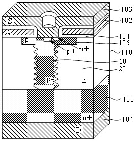
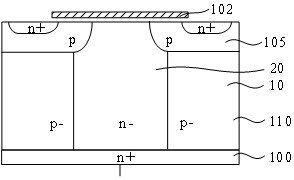
[0027] The super junction semiconductor device and its forming method of the present invention will be further described in detail below with reference to the drawings and specific embodiments. The advantages and features of the present invention will become clearer from the following description. It should be understood that the drawings in the description are all in very simplified form and use imprecise scales, and are only used to facilitate and clearly assist the purpose of illustrating the embodiments of the present invention. It will be understood that the spatially relative terms are intended to encompass different orientations of the device in use or operation in addition to the orientation depicted in the figures. For example, if a structure in the figures is inverted or otherwise positioned differently (eg, rotated), the exemplary term "on" could also include "below" and other orientational relationships.

[0028] The method for forming a super-junction semiconduct...


PUM


Abstract

The invention relates to a super junction semiconductor device and a forming method thereof. The forming method comprises the following steps of: performing an epitaxial growth process on a substrate with a first doping type for multiple times to form a plurality of sub epitaxial layers which are arranged in an overlapped manner; first doping type ion implantation is executed to form an interface compensation region located on the upper portion of a top sub-epitaxial layer in the top sub-epitaxial layer, the interface compensation region is close to an interface between the multiple sub-epitaxial layers, and the problems that the impedance between layers in the multiple sub-epitaxial layers is higher than a target value and the stability is poor can be solved; the charge balance of the N column and the P column is facilitated, and the voltage resistance and the yield of the device are improved. The super-junction semiconductor device provided by the invention is formed by adopting the forming method, the impedance between layers in the plurality of sub epitaxial layers is reduced, and the stability is improved, so that the voltage resistance and the yield of the super-junction semiconductor device are improved.

Description

technical field [0001] The invention relates to the technical field of semiconductors, in particular to a super junction semiconductor device and a forming method thereof. Background technique [0002] Semiconductor devices based on superjunction structures have been widely used in the field of medium and high voltage switching converters. Compared with traditional withstand voltage structures, superstructures form alternately arranged P-type regions (hereinafter referred to as P-pillars) in the drift region of conventional devices. ) and the N-type region (hereinafter referred to as the N-column), can make the resistivity of the drift region lower without compromising the withstand voltage capability of the device, so that the device can achieve a lower on-resistance at the same time. For super-junction semiconductor devices, the key to achieving high withstand voltage performance is to maintain the charge balance between N-pillars and P-pillars. [0003] In the manufactur...

Claims


Application Information

Patent Timeline
IPC IPC(8): H01L29/06H01L29/78H01L21/336
CPCH01L29/7827H01L29/66666H01L29/0634H01L29/0684
Inventor 梁路王东韩廷瑜
Owner SEMICON MFG ELECTRONICS (SHAOXING) CORP
Why Eureka
Try Eureka