Supercharge Your Innovation With Domain-Expert AI Agents!

Strain measurement circuit

A technology of strain measurement and circuit, applied in the direction of measuring force, measuring device, electric/magnetic solid deformation measurement, etc., can solve the problems of resolution, accuracy or temperature drift of electronic devices, etc.

Pending Publication Date: 2022-03-18
希奥检测有限公司
View PDF8 Cites 1 Cited by
  • Summary
  • Abstract
  • Description
  • Claims
  • Application Information

AI Technical Summary

Problems solved by technology

A typical problem is that the strain deformation of the entire substrate affects the resolution, accuracy or temperature drift of the electronic devices arranged on the substrate

Method used


Image

  • Strain measurement circuit
  • Strain measurement circuit
  • Strain measurement circuit

Examples


Embodiment Construction

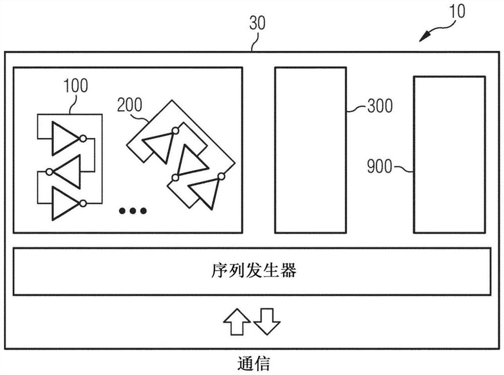
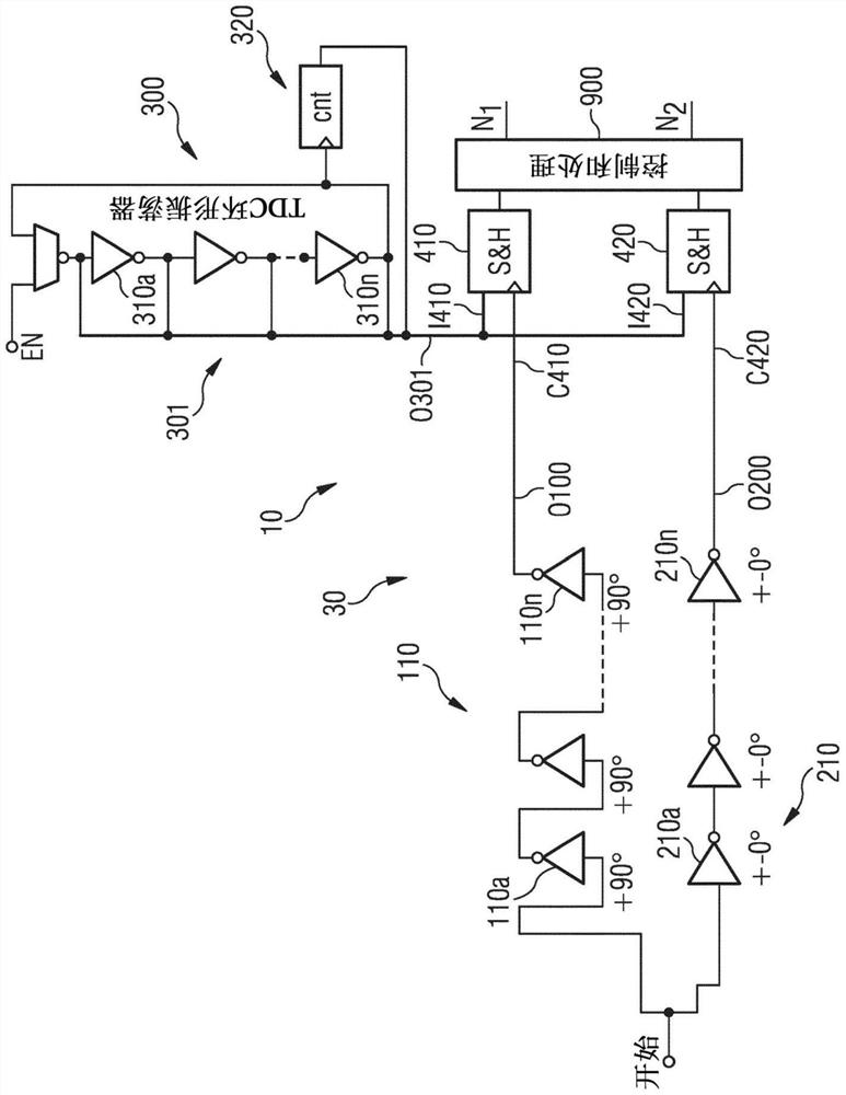
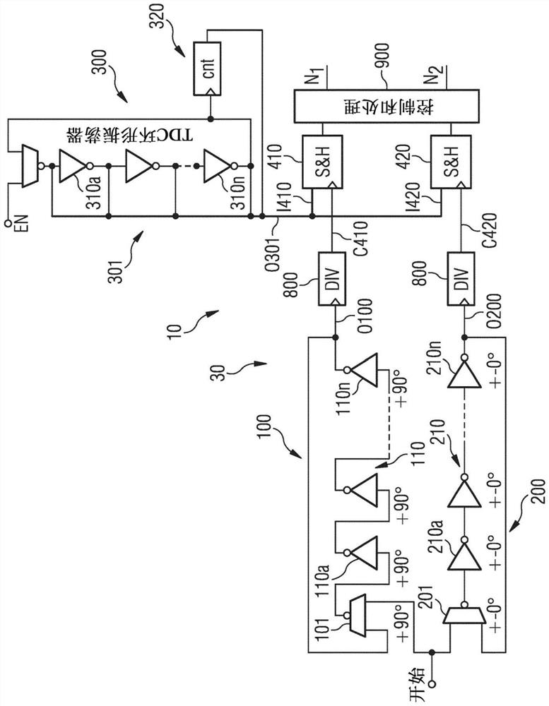
[0033] figure 1 A block diagram representing circuit blocks of the strain measurement circuit 10 is shown. The circuit 10 can be used to measure deformation of a substrate 30, such as a silicon substrate in a monolithic integrated circuit. figure 1 The embodiment of the circuit 10 shown in includes several strain-dependent ring oscillators 100, 200, a time-to-digital converter 300 and a calculation unit 900 integrated on the same substrate 30, where all components have the same deformation . according to figure 1 In the embodiment shown in the block diagram of , the circuit 10 can be configured as a monolithically integrated strain sensor capable of measuring deformation of the substrate / die 30 . Circuits can be implemented on digital standard processes, where electronics are also placed in strained regions of the die / substrate. Implementations on other processes (analog, silicon germanium) are also possible.

[0034] Circuitry 10 may be configured to measure all plane st...


PUM


Abstract

A strain measurement circuit (10) includes at least a first delay chain (110) of a plurality of delay elements (110a,..., 110n) and at least a second delay chain (210) of a plurality of delay elements (210a,..., 210n) arranged on a substrate (30). Each delay element (110a,..., 110n; 110n) of the at least one first and second delay chain (110, 210) is provided with at least one delay element (110a,..., 110n; 220a,..., 220n) depends on the strain applied to the substrate (30). The delay elements (110a,..., 110n) of the at least one first delay chain (110) have a different orientation than the delay elements (210a,..., 210n) of the at least one second delay chain (210). The circuit (10) further comprises processing circuitry (900) for determining a magnitude of strain exerted on the substrate (30) as a function of the first signal propagation delay time of the first delay chain (110) and the second delay chain (210).

Description

[0001] This patent application claims priority from European Patent Application 19191055.3, the disclosure of which is incorporated into this application by reference. technical field [0002] The present disclosure relates to a circuit for measuring strain caused by mechanical deformation of a substrate. Background technique [0003] The electronic properties of substrates on which electronic circuits are disposed or embedded, such as silicon substrates, are highly sensitive to mechanical deformations caused by strain and stress. Strain often induces parasitic effects, which degrade the performance of the electronic circuit on the substrate in terms of temperature drift, accuracy, resolution, or other parameters of the electronic circuit. Often neither the magnitude of the strain nor the direction of maximum strain is available. [0004] Strain is primarily measured with strain gauges connected to an analog-to-digital converter. Typically, strain gauge foils must be glued...

Claims


Application Information

Patent Timeline
Patent Type & Authority Applications(China)
IPC IPC(8): G01L3/04G01L1/18
CPCG01L3/045G01L1/183G01B7/18
Inventor 弗里德里希·巴恩米勒奥利弗·赫特纳弗兰克·莱姆克格奥尔格·耶德豪泽
Owner 希奥检测有限公司
Features
  • R&D
  • Intellectual Property
  • Life Sciences
  • Materials
  • Tech Scout
  • Unparalleled Data Quality
  • Higher Quality Content
  • 60% Fewer Hallucinations
Learn More